4 Layer Rogers PCB Production Record #ROG-20251219-001
| Parameter | Value | Parameter | Value |
|---|---|---|---|
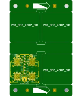
| PCB Type | Rogers PCB | Quantity | 10 pcs |
| Layers | 4 Layers | Board Type | Panel PCB |
| Dimensions | 53 x 81 mm | Copper Weight | 1oz |
| Thickness | 1.5 mm | Min Track / Spacing | 4/4mil |
| Surface Finish | ENIG (Immersion Gold) | Min Hole Size | 0.4mm |
| Solder Mask | None | Silkscreen | White |
| Material Type | Rogers/RO4350B |
This 4-layer high-frequency PCB order used a hybrid Rogers stackup with RO4003C (0.203 mm) on layers 1-2 and RO4350B (0.76 mm) on layers 3-4 to meet the 1.3–1.5 mm total thickness requirement. The 53 × 81 mm boards were built at 1.5 mm finished thickness with 0.5 oz inner copper (electroplated due to blind vias) and 1 oz outer copper. Production involved 40 pieces (10 sets) with ENIG surface finish, no solder mask, full resin plugging of 0.25 mm and 0.30 mm blind and through vias followed by plating, and V-cut + scoring separation.
Key DFM challenges included tight hole-to-hole spacing on 0.25 mm blind vias that risked breakout, V-cut proximity to copper features on the board edge, and conflicting Gerber data showing solder mask layers despite customer instructions for none. Adjustments included copper pullback on V-cuts (0.35 mm per side), removal of solder mask layers with full trace exposure under ENIG, addition of protective rings around Make points, and character printing directly on the gold surface with framed openings. Inner layer copper balancing and process edge copper were also optimized to control registration and warpage in the mixed dielectric stackup.
All hybrid stackup blind via processing issues were resolved prior to production. The order completed 100% flying probe testing with no yield loss and was delivered within the 12-day schedule.
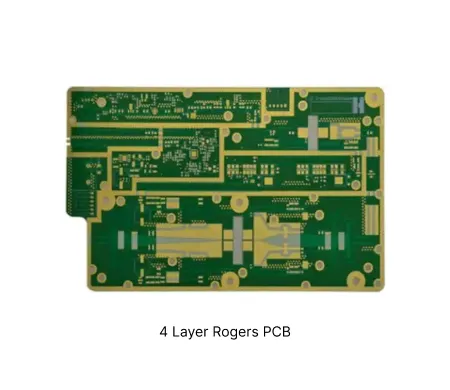
Specialized high-frequency boards combining Rogers dielectric materials with FR-4 in controlled 4-layer constructions to achieve precise impedance and signal integrity.
Master troubleshooting common Rogers PCB manufacturing challenges including drilling defects, plating adhesion, delamination, and CTE mismatch. Learn practical solutions, process adjustments, and DFM tips to improve yield for high-frequency RO4000, RO4350B, and PTFE-based boards.
| Order ID | PCB Type | Layers | Dimensions | Solder Mask | Surface Finish | Quantity | Action |
|---|---|---|---|---|---|---|---|


