High Integration, Compact Size
Leveraging microvia technology, achieves high integration and reduced dimensions, making it suitable for space-constrained applications such as mobile and wearable devices.
High-density interconnect technology ensures compact design, reliable performance, and faster signals.
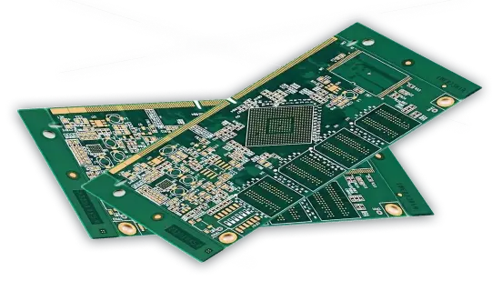
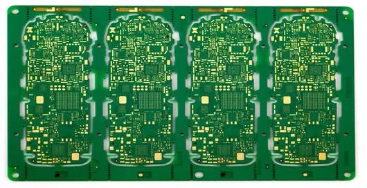
An HDI board (High Density Interconnector) is a high-density interconnection PCB that uses micro via, blind and buried via, and laser drilling technologies to achieve fine lines and spaces of less than 50 μm, allowing for high routing density. It can significantly improve signal integrity and transmission speed, supporting advanced packages such as BGA. HDI boards are widely used in 5G communications, smartphones, aerospace, and automotive electronics, making them an ideal choice for miniaturized and high-performance electronic products.
With fine-pitch routing and laser-drilled microvias, HDI technology significantly reduces overall PCB thickness and board area when compared with traditional designs. This enables a higher component density within the same physical footprint and greatly improves internal space utilization. HDI boards are an ideal choice for miniaturized products such as smartphones, wearable electronics, compact medical instruments, and other devices that require powerful functionality in very limited space. Their lightweight structure also helps manufacturers achieve slimmer profiles and improved portability.
HDI PCBs adopt shorter signal transmission paths and minimal stub lengths, which reduces signal attenuation, cross talk, and electromagnetic interference. The optimized routing architecture supports stable electrical performance even at very high frequencies. This provides strong assurance for high speed and high bandwidth applications, including 5G communication modules, radar systems, imaging sensors, and advanced automotive electronics. Users benefit from faster data throughput, lower latency, and improved reliability during continuous operation.
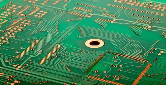
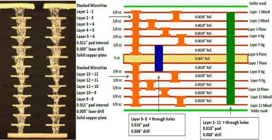
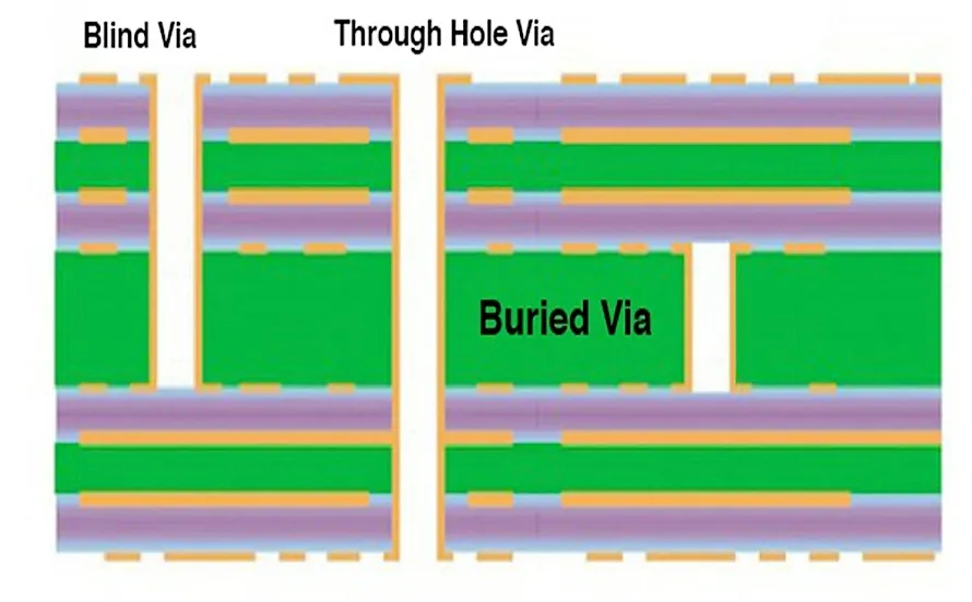
Our HDI solutions incorporate blind vias, buried vias, stacked microvias, and via in pad structures to address the increasing complexity of modern circuits. These via technologies help maximize routing space across multilayer stack ups and support components with extremely high pin counts such as BGAs and CSP packages. By improving vertical interconnections within a reduced thickness, they allow greater functional density while maintaining excellent mechanical stability and consistent electrical performance.
The closely arranged components and optimized stacked via structure in HDI PCBs enhance heat conduction paths and increase overall thermal dissipation efficiency. These features help reduce temperature rise within dense assemblies and lower the risk of heat related failures. HDI boards also provide greater resistance to thermal cycling stress and minimize potential mechanical weak points. Their stable structure makes them highly suitable for mission critical environments in aerospace systems, industrial automation equipment, defense electronics, and other applications where long term durability is essential.
Leveraging microvia technology, achieves high integration and reduced dimensions, making it suitable for space-constrained applications such as mobile and wearable devices.
Shortened signal paths reduce latency and interference, supporting high-frequency transmission, with excellent performance in 5G and other advanced communication fields.
Allows for microvias, high-precision traces, and tight spacing, ideal for advanced electronics.
Manufactured using lamination methods to lower costs, compatible with automated production, and highly competitive for large-scale manufacturing.
Uses lead-free solder to minimize resource waste, aligns with environmental standards, and supports the industry’s green transformation.
Supports multiple layers with blind/buried vias, enabling complex circuit designs while maintaining signal integrity and compact dimensions.

Used in signal boards for high-end industrial robot servo controllers and precision sensors, such as vision inspection sensors.

Applied in autonomous driving systems, cockpit domain controllers, and chassis domain controllers.

Used in smartwatches, headphones, smartphones, and foldable phones.

Used in 5G/6G base stations, RF modules, and compact communication devices for high-speed data transmission.

Applied in medical imaging systems, wearable health monitors, and precision diagnostic instruments.

Used in radar systems, avionics, and high-reliability control modules requiring superior performance and durability.
.webp)
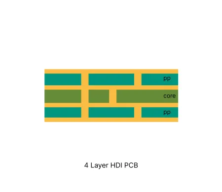
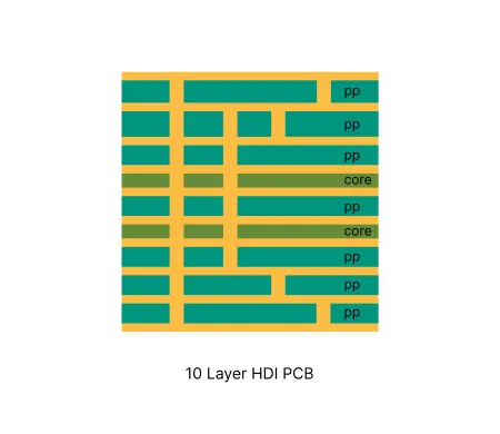
2+N+2 Structure: Includes two microvia layers on each side of the core. Offers higher wiring density and better signal integrity, ideal for 5G modules, high-speed communication, and automotive electronics.
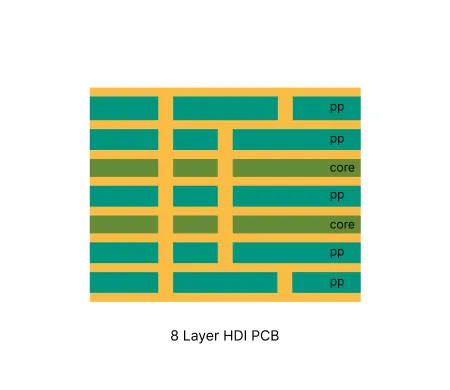
3+N+3 and Higher Structures: Advanced HDI designs with multiple stacked vias for ultra-high density interconnections. Commonly used in high-performance computing, aerospace, and military systems.
Any-Layer HDI (ELIC): Every layer can be interconnected directly through laser vias. Enables maximum routing flexibility and miniaturization, often used in flagship smartphones and advanced IoT devices.
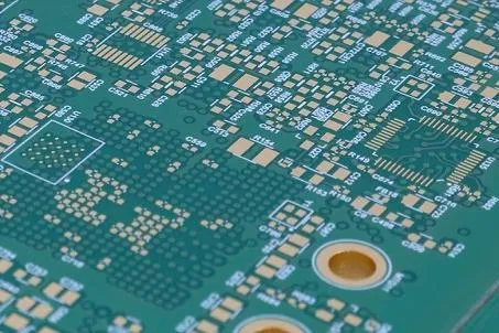
These boards deliver high routing density through laser-drilled microvias and sequential lamination while maintaining controlled production costs.
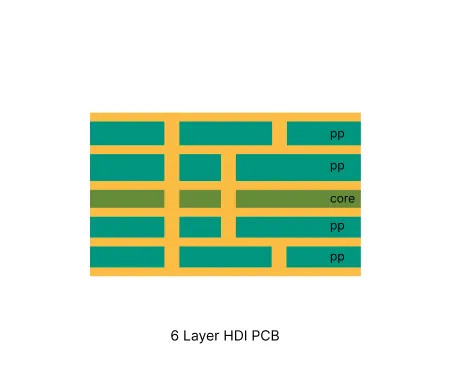
This page details production methods, specification ranges, and optimization techniques for reliable 6 layer HDI circuit boards.
These boards integrate multiple microvia layers to support complex routing and high signal density in advanced electronics.
Advanced sequential lamination and laser drilling techniques enable complex interconnects while demanding precise process control for registration and via reliability.
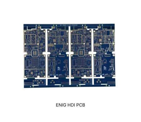
ENIG finished HDI PCBs require precise control of sequential lamination, laser drilling, copper plating, and electroless nickel immersion gold deposition to ensure via reliability and solderable surfaces.
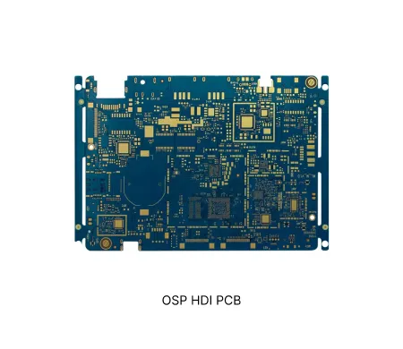
High density interconnect boards finished with OSP require controlled processes in lamination, via formation, and surface treatment to maintain solderability and reliability.
Master HDI PCB design challenges: Explore microvia rules, blind/buried vias, stackup strategies, laser drilling methods, and advanced routing for high-density interconnects. Achieve 98% yields with IPC-2226 standards—essential for 2025 AR and 5G modules.
A guide to miniaturization techniques for HDI PCB wearables. Learn microvia integration and component placement for reliable, high-density health monitors.
An engineer's guide to blind and buried vias in ultrasound PCBs. Covers laser drilling, via-in-pad, and best practices for high-density interconnect (HDI) reliability.
A1: HDI PCBs typically use high-Tg FR4, polyimide, or Rogers laminates to ensure stability under high temperatures and frequencies.
A2: Unlike traditional multilayer PCBs, HDI uses laser-drilled microvias and sequential lamination to achieve finer routing and higher interconnection density.
A3: Microvias in HDI PCBs typically range from 0.075 mm to 0.1 mm in diameter, depending on the laser drilling precision and board thickness.


