High Current Carrying Capacity
Thick copper layers can handle higher currents (e.g., tens of amperes in power modules), reducing resistive loss and the risk of overheating, and preventing circuit damage.
Handle higher currents, dissipate heat faster, and deliver unmatched reliability.
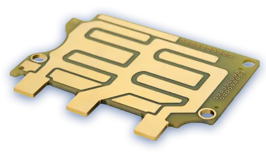
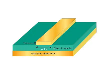
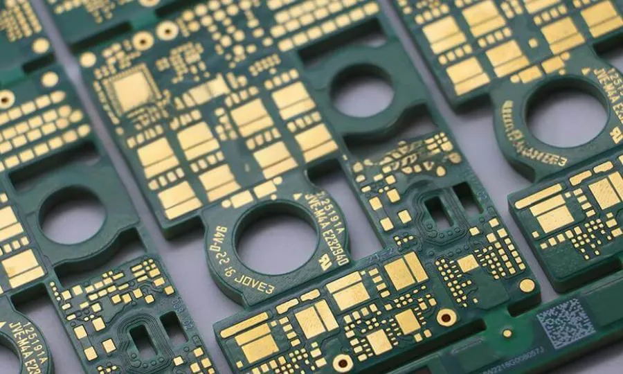
Heavy Copper PCBs are printed circuit boards manufactured with extra-thick copper layers (typically ≥3 oz/ft2, or over 105 μm) on substrates such as FR-4. Compared to standard PCBs (with 1–2 oz copper), heavy copper PCBs have significantly thicker copper layers, providing enhanced current-carrying capacity and thermal performance. They are widely used in new energy vehicles, high-power power supplies, industrial control systems, and other applications, making them the preferred choice for high-power, high-stability designs.
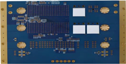
A 2-layer printed circuit board with relatively thick copper and ENIG (Electroless Nickel Immersion Gold)surface finish, widely used in the electronics industry.
Designed for high-power, high-current, and high-heat-dissipation electronic applications.
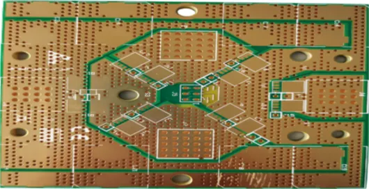
A 2-layer thick copper PCB designed for medical instruments where reliability and precision are critical.
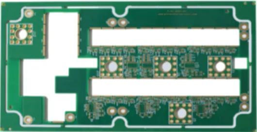
A key foundational component forindustrial control, automotive electronics, and energy equipmentapplications.
Thick copper layers can handle higher currents (e.g., tens of amperes in power modules), reducing resistive loss and the risk of overheating, and preventing circuit damage.
Copper's high thermal conductivity quickly transfers heat, lowering the operating temperature of electronic components and improving system stability and lifespan.
Heavy copper PCBs resist warping and delamination under repeated thermal cycles, ensuring long-term stability and reliability in power electronics, industrial, and aerospace applications.
Thick copper layers provide greater resistance to vibration and impact, making them suitable for harsh environments such as automotive and industrial equipment.
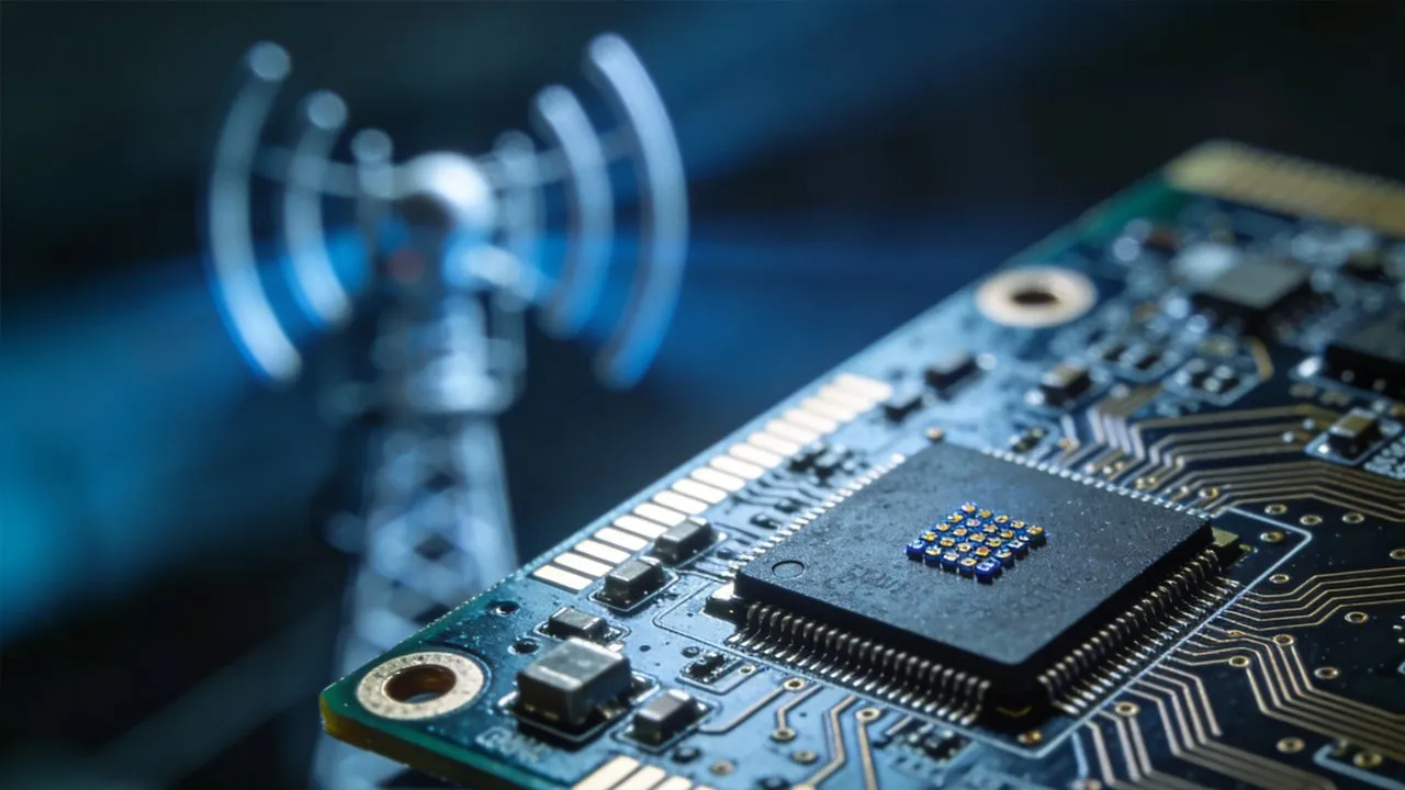
Reduces signal loss and crosstalk in high-frequency or microwave circuits, making it ideal for communication base stations, radar systems, and other high-frequency applications.
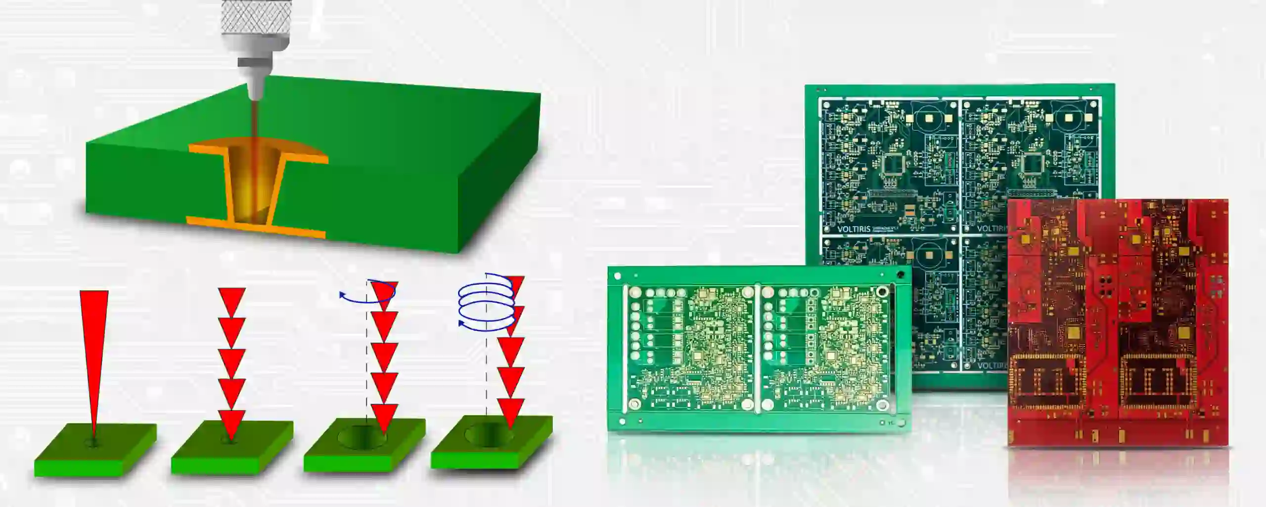
Can be fabricated using standard and advanced PCB techniques, including multi-layer lamination, SMT assembly, and precision etching, enabling complex circuit designs without compromising performance.
AIVON provides PCBs for a motor controller uses a heavy-copper PCB to manage high currents, delivering precise power pulses that control motor speed, torque, and position with exceptional accuracy.

For an ADAS module, AIVON developed HDI PCBs with controlled impedance and high-speed signal routing to support radar and camera data processing. The design achieved excellent EMI shielding and consistent signal transmission in safety-critical environments.

PCBs enable advanced LED lighting systems in modern vehicles, from adaptive headlights to dynamic tail lights, all requiring robust boards with excellent thermal management for longevity and reliability.

The primary power conversion board in a 3kW server power supply uses a heavy-copper PCB to efficiently handle high-current 48V to 12V conversion with minimal losses and optimal thermal performance.

AIVON supplied a 12-layer polyimide PCB with high Tg material and ENIG surface finish for an aircraft avionics control system. The board achieved excellent thermal endurance and signal stability, ensuring reliable flight control performance under fluctuating temperatures and vibration.

Electronic chart display and AIS transponder systems rely on multi-layer PCBs with optimized RF characteristics and humidity protection to ensure reliable operation in the challenging marine atmosphere.
Key aspects of heavy copper construction include:
Thick Copper Layers: Provide high current carrying capacity and reduce resistive loss.
Robust Base Material: Ensures mechanical strength and dimensional stability.
Advanced Plating & Surface Finish: ENIG or HASL finishes protect the copper and ensure reliable soldering.
Thermal and Electrical Reliability: Optimized for industrial, automotive, military, and aerospace applications where high power and durability are required.
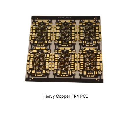
Heavy copper FR4 combines thick copper layers with standard FR4 materials to deliver high current capacity and improved thermal performance in power electronics.
 Heavy-Copper PCB
Master heavy copper PCB design with this comprehensive guide. Learn critical design rules, thermal management strategies, current carrying capacity calculations, via design, and how heavy copper delivers superior reliability compared to standard PCBs.
 Power Electronics
Master the heavy copper PCB manufacturing process with this detailed step-by-step guide. From material selection and heavy copper plating to differential etching and quality control — plus key insights on when to choose heavy copper over standard PCB.
 Rogers PCBs
Explore the comprehensive world of Rogers PCB applications. This guide covers material properties, engineering benefits, and technical insights for implementing Rogers laminates in advanced electronic systems.
A1: The right copper thickness depends on current requirements, thermal management, and mechanical durability. Higher currents or high-power applications require thicker copper to reduce resistive loss and prevent overheating. For most industrial and automotive applications, copper thickness ranges from 3 oz to 10 oz, while extremely high-current applications may need up to 20 oz.
A2: Most heavy copper PCBs use FR-4, metal-core substrates, or high-TG materials to maintain structural stability under high temperatures and currents.
A3: Choose heavy copper PCBs when your application requireshigh current, superior heat dissipation, or mechanical robustness. Standard PCBs are suitable forlow-power, low-heat applications.
A4: The thick copper traces act as built-in?heat spreaders, reducing thermal strain on components and significantly extending the lifespan of?high-voltage electronics.


