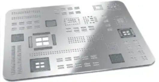
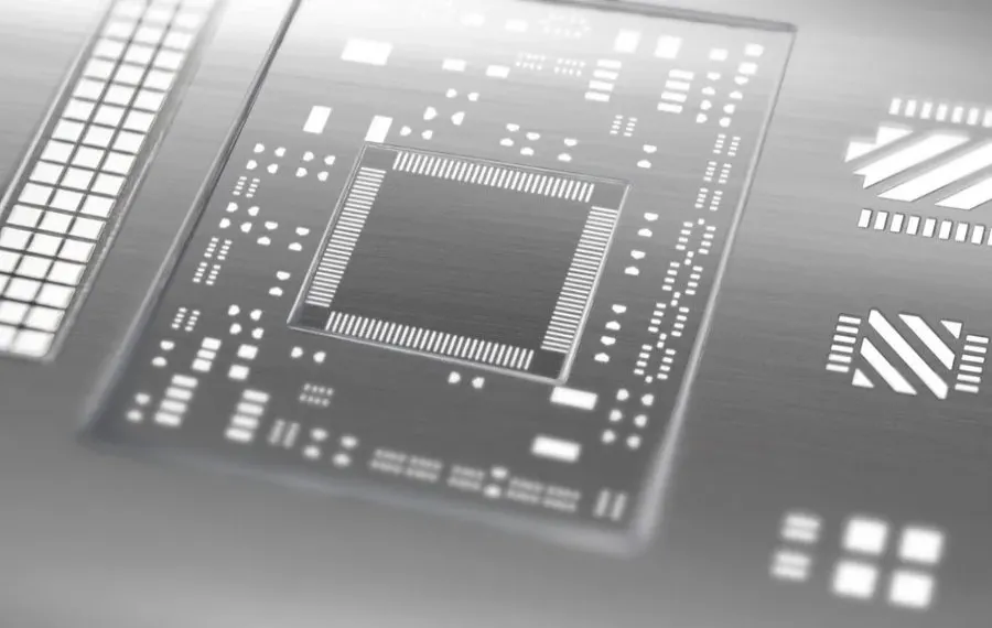
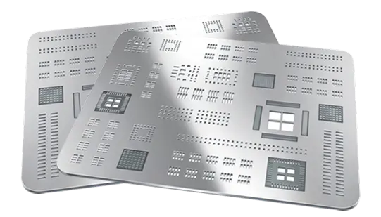
Select stencil thickness based on pad size and component type. Thinner stencils suit ultra-fine-pitch components, while thicker stencils provide more solder paste but may increase bridging risk. Aperture size is generally 80–100% of the pad area. Rectangular apertures are used for ICs, round or oval for passives, and chamfered for BGAs. For fine-pitch pads, reduce aperture area to prevent solder bridging.
Choose standard, step, or patterned apertures to control solder volume. Large thermal pads benefit from a grid of smaller openings to ensure proper solder release and reduce voids. Align apertures with component terminals for consistent paste deposition.
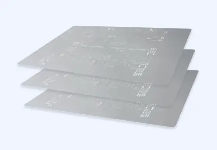
Proper paste volume is essential to avoid open joints or bridging. Adjust aperture size or stencil thickness and apply reduction factors for fine-pitch components. Use stainless steel or electroformed stencils for precise openings and maintain cleanliness for consistent results.
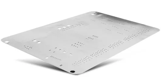
Coordinate stencil design with PCB layout, including component spacing and fiducials, to ensure accurate alignment and uniform paste printing. Validate designs using solder paste inspection and adjust if defects are observed.
.webp)