










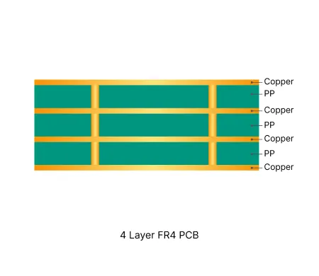
4 Layer FR4 PCB
Discover how AIVON manufactures 4 Layer FR4 PCBs, including multilayer stackup design, layer alignment control, fabrication processes, manufacturing challenges, and real production experience from customer orders.
AIVON provides custom 4 layer PCBs manufacturing with optimized stackup design, controlled impedance, and reliable signal integrity for high-speed, compact, and multifunctional electronic applications.


A 4-layer PCB is a multilayer printed circuit board made up of four copper layers separated by dielectric materials and laminated into a single board. A typical 4-layer PCB stackup may include two signal layers and dedicated ground and power planes, although the exact layer configuration can be customized according to routing, power distribution, impedance. It's widely used in complex electronic systems where stable power distribution, signal integrity, and compact design are essential.
AIVON's 4-layer PCBs are engineered with precise stackup design and impedance control to ensure reliability in high-speed and high-frequency applications.


A 4 layer PCB stackup defines how the four copper layers, dielectric materials, and core are arranged within the board. A typical configuration uses two outer signal layers with dedicated ground and power planes between them, but the layer arrangement can be adjusted according to routing density, impedance requirements, power distribution, and application needs. Proper stackup planning helps establish consistent reference planes, maintain controlled impedance, and provide predictable signal return paths for high-speed circuits. The guide covers common 4 layer stackup configurations, including signal, ground, power, and signal layer arrangements, as well as the role of core and prepreg materials.

Routing a 4-layer PCB requires more than simply connecting components. The layer structure provides additional routing space, dedicated power and ground planes, and better control of signal return paths. This practical guide explains how to plan component placement, route power and ground, keep signal traces short, manage vias, and separate analog and digital signals. It also covers common routing challenges such as crosstalk, plane interruptions, and power distribution, with a microcontroller circuit as a practical example. The article also highlights how stackup selection affects routing efficiency, signal integrity, and overall board performance. By considering layer assignments early, designers can create clearer signal paths and reduce unnecessary vias and routing conflicts.
Discover how AIVON manufactures 4 Layer FR4 PCBs, including multilayer stackup design, layer alignment control, fabrication processes, manufacturing challenges, and real production experience from customer orders.
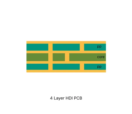
Discover how AIVON manufactures 4 Layer HDI PCBs, including microvia structures, fine-line routing requirements, sequential lamination processes, manufacturing challenges, and real production experience from customer orders.
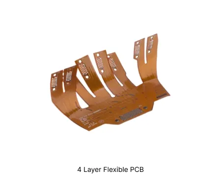
Discover how AIVON manufactures 4 Layer Flexible PCBs, including multilayer flexible circuit structures, layer alignment control, bending performance, manufacturing challenges, and real production experience from customer orders.
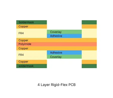
Discover how AIVON manufactures 4 Layer Rigid-Flex PCBs, including rigid and flexible layer integration, mechanical reliability requirements, fabrication processes, manufacturing challenges, and real production experience from customer orders.
| Order ID | PCB Type | Layers | Dimensions | Solder Mask | Surface Finish | Quantity | Action |
|---|---|---|---|---|---|---|---|
| Loading... | |||||||
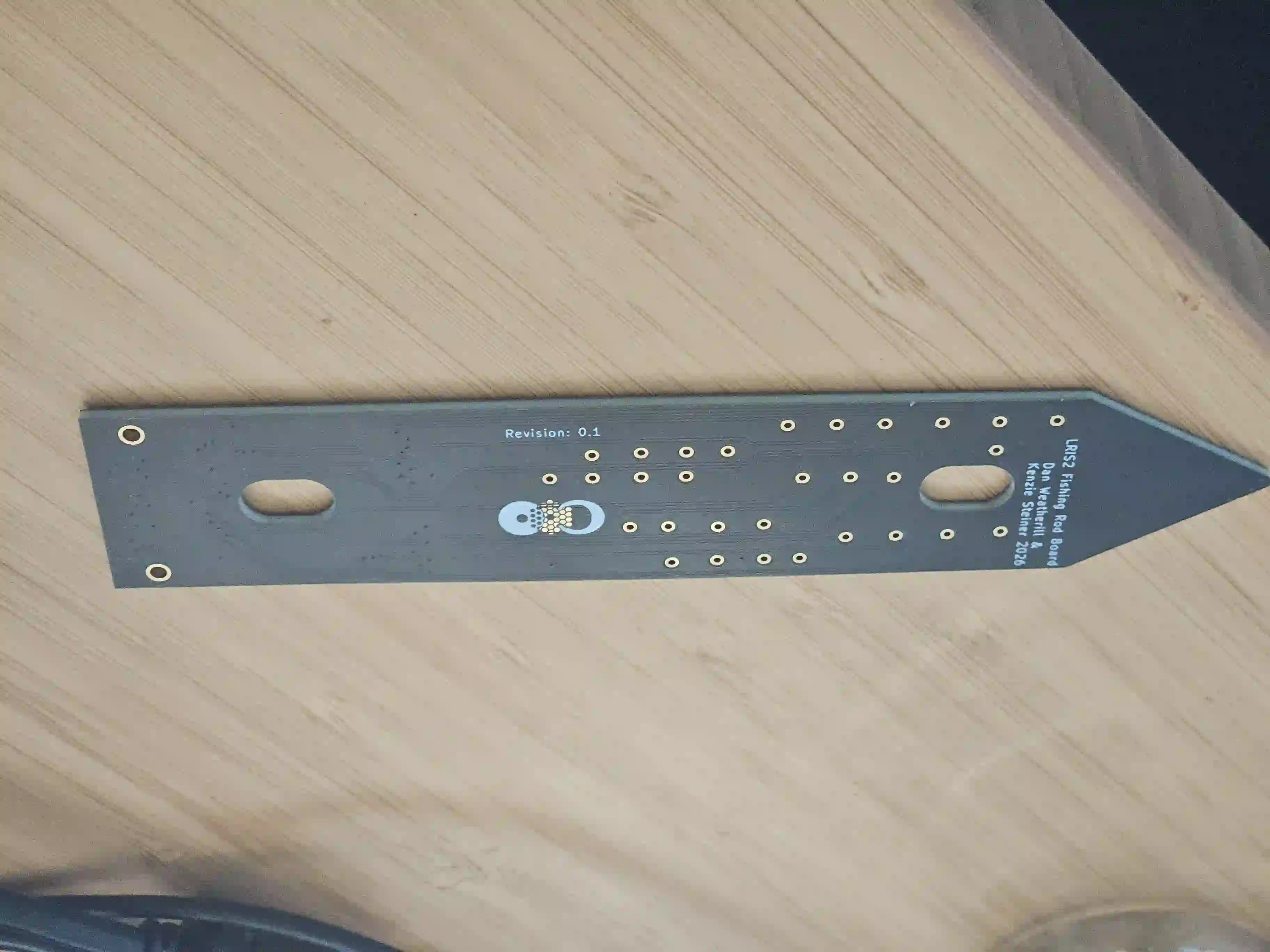
 AI*****S5

FR-4, 4-Layer, 25mm * 124mm, Matte Black, ENIG (Immersion Gold), 10 PCS
Excellent quality as always from Aivon and fast processing time
See how this PCB was manufactured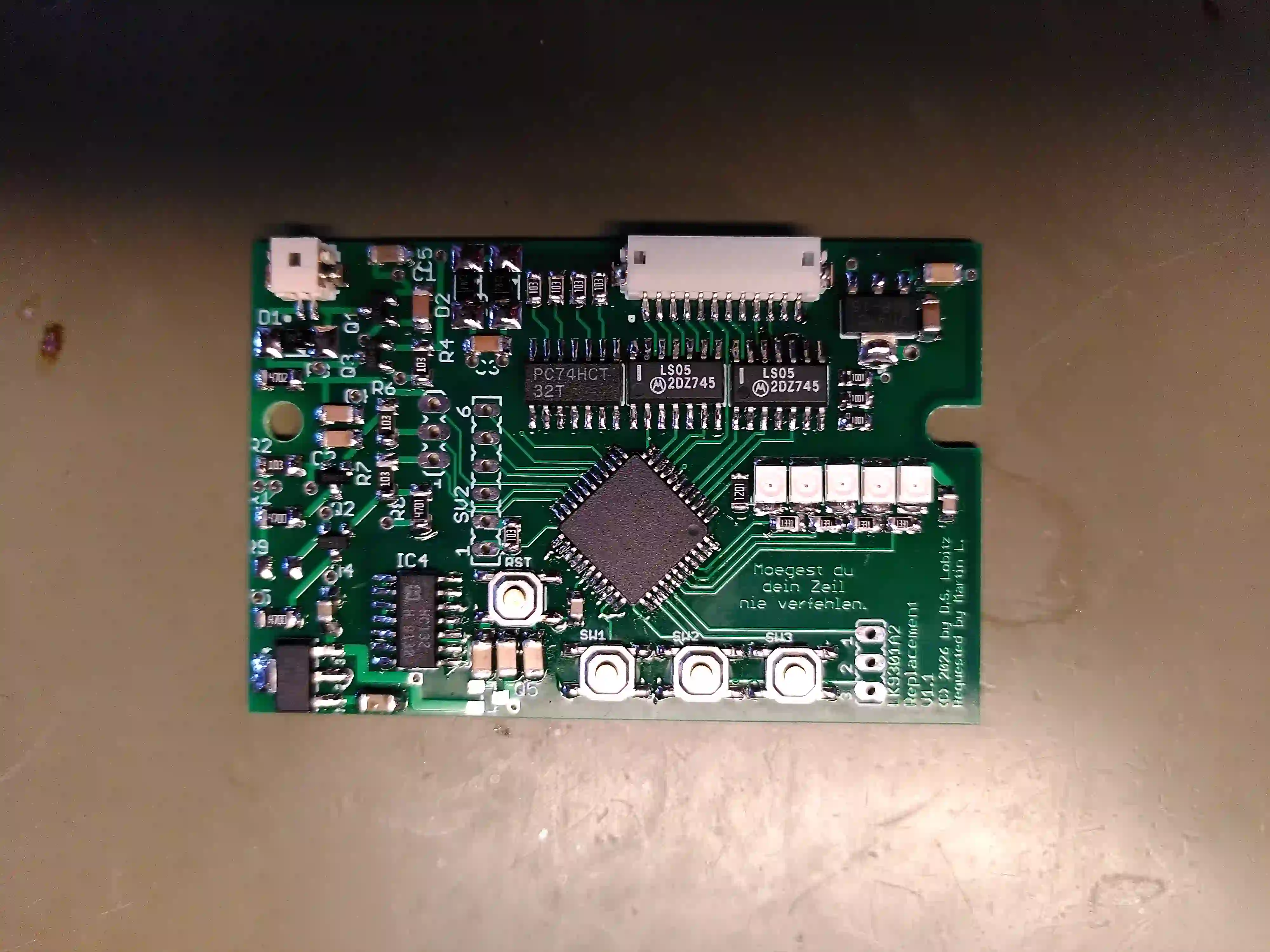 AI****9A

FR-4, 4-Layer, 67mm * 43.7mm, Green, HASL Lead Free, 10 PCS
The quality of the PCBs is outstanding, especially considering the highly competitive pricing. Communication with my account manager is always excellent, helpful, and highly efficient. Furthermore, despite shipping from overseas, the delivery arrived within just three working days. Finally, the web interface strikes a perfect balance: it is very intuitive and well-structured for quick tasks, yet it provides experienced users with all the advanced features and technical capabilities an engineer could ask for.
See how this PCB was manufactured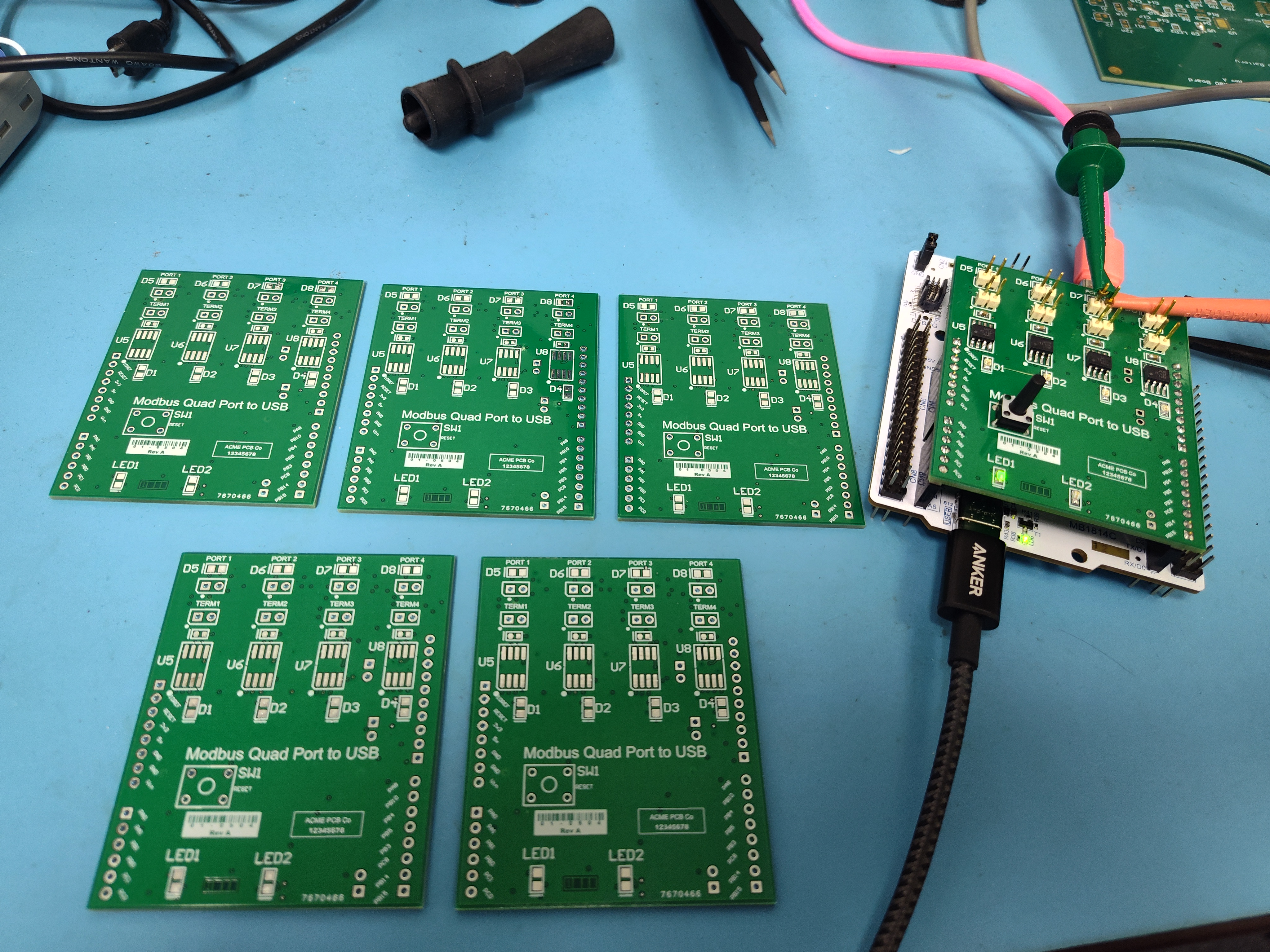 AI****2A
FR-4, 4-Layer, 54.1mm * 66.04mm, Green, HASL Lead Free, 5 PCS
The boards look good and had no problem during assembly. They arrived quicker than expected. Six boards arrived even though only five were ordered. No problems with this order, will order again.
See how this PCB was manufactured

FR-4, 4-Layer, 150mm * 100mm, Green, HASL Lead Free, 5 PCS
Hi, I finally completed my project! I was surprised by the quality/price ratio of the board. I ask you produce a 4 layer board for my 5.1 audio system and it was perfect. Surely in the future I' ll contact you again!
See how this PCB was manufactured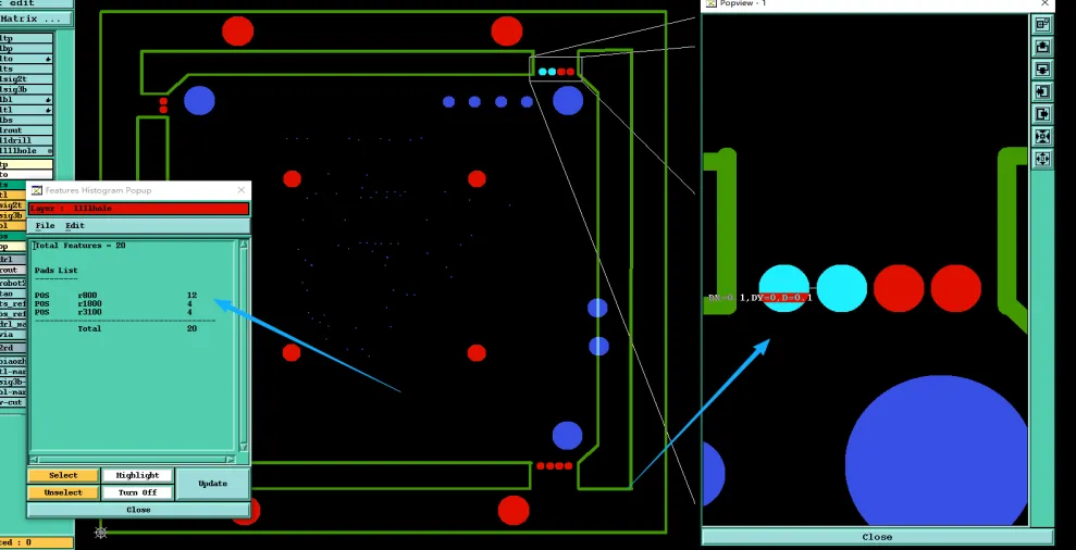 PCB Manufacturing Defects
This 4 layer FR4 PCB DFM review identifies risks in breakaway tab design and silkscreen placement. Improve production yield and assembly quality with these practical technical tips.
 Solder Mask
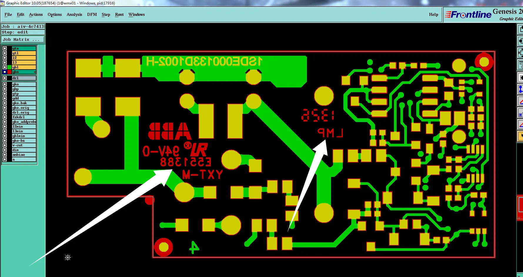
CAM review of a small 4-layer ENIG board found no silkscreen layer and insufficient solder-mask space for required sequential IDs and UL marks. Marks were relocated to clear top-side areas to meet IPC-4552 without reducing clearance.
 PCB Reliability
Senior PCB CAM engineer shares a real 4-layer HDI PCB engineering case study. Discover key DFM issues including stackup thickness deviation, 1.35mm countersink hole processing on copper, core material availability challenges, and strict drill tolerances. Learn how our team resolved these manufacturing risks through EQ clarification to prevent warpage, plating defects, and production delays. Essential DFM insights for PCB designers.

4-layer PCBs provide a practical balance of routing capacity, compact design, and electrical performance for consumer electronics. They are widely suited to products such as smart home devices, wearables, audio equipment, displays, and portable electronics. Additional routing layers help accommodate more components within limited board space, while dedicated power and ground planes support stable power distribution and signal integrity.

Medical electronics require stable electrical performance, compact layouts, and reliable PCB manufacturing. 4-layer PCBs provide additional routing space and dedicated power and ground layers, making them suitable for monitoring equipment, diagnostic devices, portable medical electronics, and control modules. The multilayer structure helps manage signal paths and power distribution within compact board dimensions.

4-layer boards can be used in control modules, infotainment systems, sensor interfaces, lighting electronics, and other vehicle electronics. Separate routing and plane layers provide more flexibility for managing power and signal paths, while the additional layer capacity supports higher component density than conventional 2-layer boards. Consistent fabrication and material selection are important for achieving reliable performance in automotive applications.

Telecommunication equipment often requires efficient signal routing, stable power distribution, and controlled electromagnetic performance. A 4-layer PCB provides additional routing capacity while allowing power and ground planes to be incorporated into the stackup. This structure can support communication modules, networking equipment, wireless devices, and signal interface boards.

A 4-layer PCB board structure provides additional routing space and dedicated power and ground layers, helping organize these different circuit functions within a compact board. It can be applied to PLC modules, motor control systems, automation equipment, monitoring units, and industrial interfaces. Proper stackup design, signal routing, power distribution, and grounding are essential for maintaining stable operation and reliable connections in industrial environments.
AIVON provides controlled multilayer PCB manufacturing with consistent layer alignment, drilling, plating, and lamination processes for reliable 4-layer board production.
For designs with high-speed or sensitive signals, AIVON supports controlled impedance requirements through appropriate stackup planning, trace dimensions, and manufacturing control.
Choose from different PCB materials, copper weights, surface finishes, and stackup configurations to match electrical, mechanical, and application-specific requirements.
From initial prototypes to repeat production, AIVON supports efficient manufacturing workflows to help reduce turnaround time while maintaining production consistency.
Using high-TG FR4 or hybrid materials, our 4-layer PCBs provide excellent heat resistance and structural reliability under continuous high-load operation.
AIVON's engineering team can review Gerber files and manufacturing requirements, helping identify potential fabrication issues and improve design manufacturability before production.
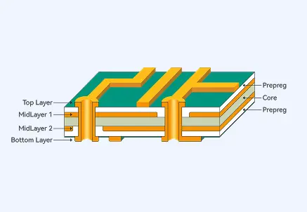
A well-planned 4-layer PCB layout uses each layer strategically to improve routing efficiency, power distribution, and signal integrity. In addition to arranging signal traces, designers need to consider how power and ground planes are positioned within the stackup.
A properly designed plane structure can provide shorter return paths, reduce interference, and support more stable power delivery. Understanding the relationship between signal layers, power planes, and ground planes is an important part of designing a reliable 4-layer PCB. Learn more about practical power and ground plane design considerations in 4-layer PCB layouts.
A1: A 4-layer PCB is worth considering when a design requires more routing space, dedicated power and ground planes, controlled impedance, or better control of signal return paths. It is commonly used for denser layouts, high-speed interfaces, mixed-signal circuits, and designs with tighter EMI requirements. For simple, low-density circuits, a 2-layer PCB may still be sufficient.
A2: 1.6 mm is a commonly used finished thickness for 4-layer PCBs, but the appropriate thickness depends on the application, mechanical requirements, stackup, impedance targets, and manufacturing specifications. Thinner or thicker constructions can also be produced when the design requires them.
A3: Key factors include proper layer stackup, trace width control, grounding strategy, and differential pair design to maintain performance and minimize crosstalk. Designers should also consider thermal management, EMI, trace width and spacing, and manufacturability. A well-planned 4-layer layout assigns each layer a clear function and maintains continuous reference planes where needed.
A4: A 4-layer PCB generally costs more to manufacture than a 2-layer PCB because it requires additional copper layers, dielectric materials, and lamination processes. However, the higher layer count can reduce routing complexity, board size, and the need for design compromises. For more complex circuits, these benefits can make a 4-layer design practical despite the higher fabrication cost.
A5: A properly designed 4-layer PCB can provide more predictable signal behavior by placing signal layers close to continuous reference planes. This helps provide shorter return paths and makes impedance-controlled routing easier. However, simply increasing the layer count does not automatically improve signal integrity. Stackup, routing, plane continuity, and via transitions still need to be properly designed.
A6: Yes. A 4-layer PCB can support controlled impedance when the stackup, dielectric thickness, copper weight, trace geometry, and target impedance are properly defined. The manufacturer should confirm the actual stackup and adjust trace dimensions based on the selected materials and fabrication process. This is particularly important for high-speed and differential signals.


