Expert Engineering Support
AIVON’s experienced engineers provide one-on-one DFM and stackup design assistance to ensure your rigid-flex PCB meets both mechanical and electrical performance requirements.
AIVON offers precision-engineered 8-layer PCBs with optimized signal routing, controlled impedance, and multilayer thermal management for high-speed and high-density electronics.
.webp)
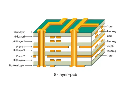
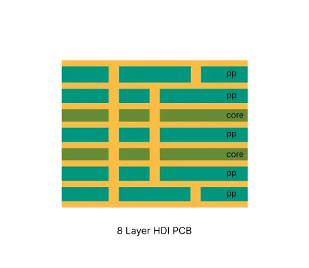
An 8-layer PCB is a multilayer printed circuit board that consists of eight conductive copper layers, typically arranged with alternating signal and plane layers for power and ground. This configuration allows for high-density routing, improved signal integrity, and reduced electromagnetic interference (EMI), making it suitable for complex, high-speed electronic designs.
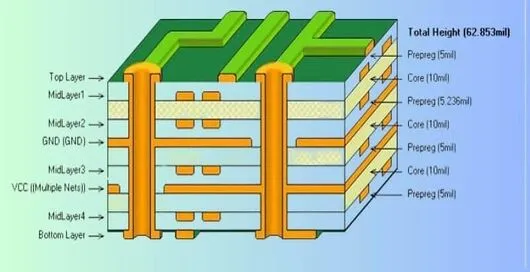
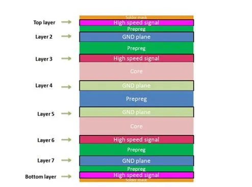
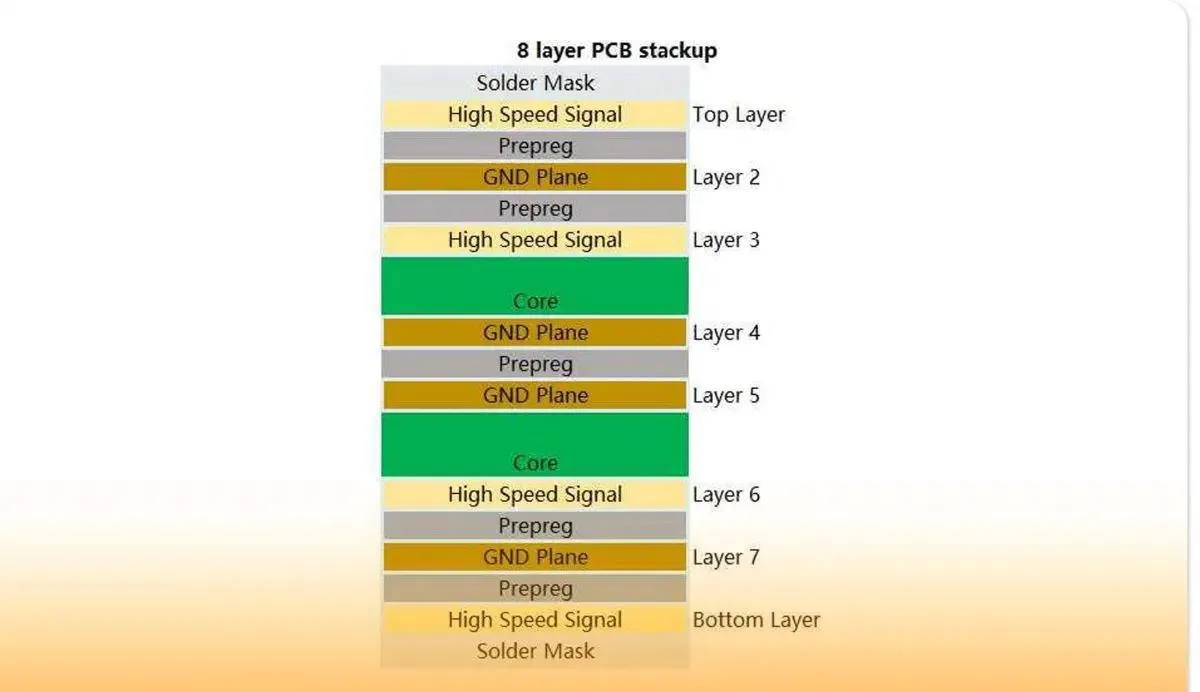
AIVON’s 8-layer PCBs feature a carefully balanced layer structure, with signal, power, and ground layers strategically arranged to reduce electrical noise and enhance mechanical stability. This thoughtful layer distribution simplifies complex routing and improves overall circuit reliability. By providing clear separation between high-speed signals and power planes, these PCBs support advanced designs while maintaining consistent performance across all layers. The architecture is particularly suitable for high-density electronic systems in telecommunications, computing, and industrial automation.

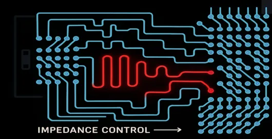
The multilayer configuration allows designers to route a high density of traces efficiently while keeping signal paths short. Controlled impedance traces are meticulously designed to prevent signal reflection, timing delays, and cross-talk. This ensures reliable data transmission even in high-speed and high-frequency circuits. Applications such as 5G communication modules, server boards, and automotive control units benefit from enhanced routing efficiency and reduced design complexity.
Dedicated ground planes in the inner layers act as effective shields against electromagnetic interference. When combined with impedance-controlled routing, this configuration ensures stable signal integrity for high-speed digital circuits and RF applications. Engineers can rely on consistent signal quality in environments that are sensitive to noise, such as communication equipment, radar systems, and precision instrumentation.
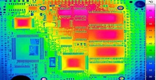
Thermal vias, optimized copper planes, and layer stacking strategies enhance heat dissipation across the PCB. This keeps critical components within safe operating temperatures, maintaining stable electrical performance under high power loads. Effective thermal management extends the lifespan of components and reduces the risk of overheating in demanding applications, including industrial machinery, aerospace systems, and high-performance computing devices.
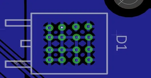
AIVON utilizes through-hole, blind, and buried vias to interconnect PCB layers efficiently. The selection of via type is based on current-carrying requirements, signal speed, and manufacturability considerations. This versatile approach ensures reliable vertical interconnections while supporting complex high-pin-count components such as BGAs and CSPs. It allows engineers to achieve dense designs without compromising electrical performance or long-term reliability.
AIVON’s experienced engineers provide one-on-one DFM and stackup design assistance to ensure your rigid-flex PCB meets both mechanical and electrical performance requirements.
Equipped with precision laser drilling, automated lamination, and high-speed routing machines to guarantee tight tolerances and superior interlayer bonding.
Supports a wide range of materials, including Polyimide, FR4, and hybrid Rogers composites, for optimized flexibility and signal integrity.
Each PCB undergoes multi-stage inspection—AOI, X-ray, E-test, and bend testing—to ensure flawless reliability and long-term durability.
Whether you need small prototypes or full-scale mass production, AIVON’s flexible manufacturing lines can adapt to your project needs efficiently.
With fast lead times and international logistics support, AIVON ensures your rigid-flex PCB projects are delivered on time, every time.

AIVON provided a 10-layer HDI PCB for a global smartphone brand, featuring fine-line circuitry, blind and buried vias, and high-speed signal routing. The board was optimized for compact design and thermal management, ensuring stable performance even under heavy processing loads.

For an ADAS module, AIVON developed HDI PCBs with controlled impedance and high-speed signal routing to support radar and camera data processing. The design achieved excellent EMI shielding and consistent signal transmission in safety-critical environments.

AIVON supplied a 6-layer multilayer PCB for a portable patient monitoring device. The board integrated analog sensors, ADCs, and wireless modules while maintaining signal integrity and low noise, enabling accurate real-time vital signs measurement.
AIVON supplied a 10-layer high-frequency PCB using Rogers + FR4 hybrid material, designed for low signal loss and stable impedance in 5G base station systems. The optimized layer stackup and precise drilling ensured superior RF performance under high data transmission rates.
AIVON provides PCBs for a motor controller uses a heavy-copper PCB to manage high currents, delivering precise power pulses that control motor speed, torque, and position with exceptional accuracy.
These boards integrate multiple microvia layers to support complex routing and high signal density in advanced electronics.
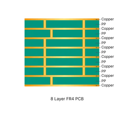
These multilayer boards support dense circuitry with eight copper layers while maintaining controlled impedance and thermal performance.
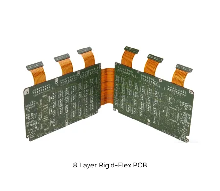
These boards combine multiple rigid zones with flexible interconnects. The construction supports complex routing in space-constrained dynamic applications.
 8-Layer PCB
Discover expert PCB design for power electronics using 8-layer boards optimized for demanding high-current and high-voltage applications. Learn key considerations for trace sizing, creepage, layer stackup, and manufacturing to minimize noise, heat, and risk while maximizing performance.
 PCB Stackup
Delve into the world of 8-layer PCBs, understanding their structure, high-performance applications, critical design considerations, and advanced manufacturing processes for complex electronics.
 PCB Cost
Discover the main 8-layer PCB cost drivers—from materials and fabrication to assembly—that directly impact your multilayer pricing. Get practical strategies for cost-effective 8-layer PCB design, avoid common pitfalls, and achieve balanced budgets. Request your instant quote from AIVON today.
A1: Prototype orders can be completed within 5–7 working days, while mass production typically requires 10–15 days depending on complexity.
A2: Yes. AIVON’s engineering team assists customers with DFM analysis, stackup design, and impedance modeling to ensure manufacturability and performance consistency.
A3: AIVON’s 8-layer PCB typically has a standard thickness of 1.6 mm, commonly used for multilayer designs. Depending on material selection, copper weight, and stack-up requirements, AIVON can also provide custom thickness options such as 2.0 mm or 2.4 mm to meet specific electrical or mechanical needs.
A4: An 8-layer PCB offers greater routing density, enhanced EMI/EMC control, better signal integrity, and superior thermal performance for complex designs.


