Why 8-Layer PCBs Excel in High Power PCB Design?
For power electronics applications that necessitate the management of substantial currents and voltages, an 8-layer Printed Circuit Board (PCB) frequently emerges as the optimal solution. These multi-layered boards inherently offer an enhanced capacity for accommodating intricate circuits, superior thermal management capabilities, and improved signal integrity—qualities that make them exceptionally well-suited for demanding applications like power converters, complex MOSFET layouts, and robust IGBT configurations.
Compared to boards with fewer layers, an 8-layer PCB provides distinct advantages in scenarios involving high power. The multiple layers allow for the strategic allocation of dedicated planes for power distribution, grounding, and signal routing. This segregation effectively minimizes electrical noise and significantly boosts operational efficiency. For example, in high-current scenarios, the generous trace widths and dedicated power planes within an 8-layer PCB can comfortably manage currents exceeding 10A without experiencing problematic voltage drops. Similarly, in high-voltage designs, the additional layers facilitate better spacing and electrical isolation, thereby substantially reducing the risk of arcing or dielectric breakdown, particularly when dealing with potentials above 500V. This inherent robustness positions 8-layer PCBs as a primary choice for sophisticated power converters and critical layouts involving power MOSFETs and IGBTs.
Current Density and Copper Weight Selection
Current density is one of the most important considerations in high current PCB design. Excessive current density leads to overheating, voltage drop, and premature failure.
According to IPC-2221 standards, the maximum current-carrying capacity depends on copper thickness, trace width, and acceptable temperature rise. For high-power applications, 2oz or 3oz copper is typically used on power layers.
Copper Weight Selection Guide:
| Copper Weight | Recommended Current (10°C rise) | Typical Trace Width for 30A | Best Used For |
|---|---|---|---|
| 1 oz | Up to 15A | 120 mils | Low power |
| 2 oz | 25–40A | 80 mils | Most power electronics |
| 3 oz | 45–70A | 55 mils | High current applications |
| 4 oz | 70A+ | 40 mils | Extreme power designs |
For most 8-layer PCB power designs, using 2oz copper on external layers and 3oz on internal power planes provides an excellent balance between performance, cost, and manufacturability. Always verify your design using IPC-2152 calculators or field solver tools.
Key Considerations for High-Current 8-Layer PCB Design for Power Electronics
Crafting an 8-layer PCB for applications involving high currents demands meticulous planning to safeguard both operational safety and performance. Unmanaged high currents can lead to excessive heat generation and detrimental voltage drops. Here are critical factors to integrate into your high-current 8-layer PCB design:
Trace Dimensions and Copper Weight
To effectively manage higher currents, it is imperative to use wider and thicker traces. For instance, a trace intended to carry 10A might require a minimum width of 100 mils with a copper thickness of 2 oz/ft² to adequately minimize electrical resistance and prevent excessive heat buildup.
Power Plane Allocation and Thermal Management
Dedicate at least two internal layers specifically as power planes. This strategic allocation ensures current is distributed uniformly across the board, which in turn reduces impedance and guarantees a stable power supply. Given that high currents inevitably generate heat, it's crucial to integrate thermal vias and strategically placed heat sinks near high-current components to facilitate efficient heat dissipation. The goal for critical areas should be a thermal resistance below 1°C/W.
Strategic Component Placement
Position high-current components as close as possible to the dedicated power planes. This minimizes trace lengths, thereby reducing resistive losses. Grouping related components can also help avoid creating long, high-current paths, further enhancing efficiency and thermal performance.
Strategies for High-Voltage 8-Layer PCB Design
High-voltage applications introduce a unique set of challenges, including the inherent risks of electrical breakdown and electromagnetic interference. An 8-layer PCB high-voltage design must therefore prioritize safety and effective electrical isolation. Here’s a strategic approach to consider:
Creepage and Clearance Standards
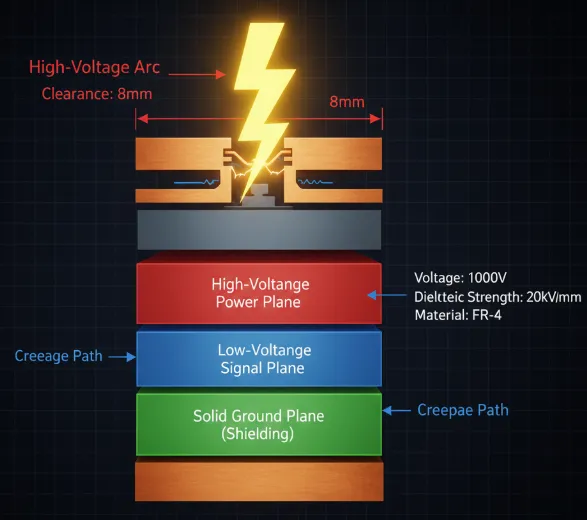
Maintaining adequate spacing between high-voltage traces is critical to prevent dangerous arcing. For voltages around 1kV, a clearance of at least 8mm is often recommended, though this can vary based on the specific dielectric material used and environmental conditions.
Layer Isolation and Dielectric Strength
Utilize internal layers to create clear separation between high-voltage circuits and sensitive low-voltage signals. This physical isolation effectively minimizes crosstalk and significantly enhances overall safety. Furthermore, selecting a PCB material with a high dielectric strength, such as FR-4 with a breakdown voltage of 20kV/mm, is essential to reliably withstand high potentials without failure.
Robust Ground Planes
Implement solid ground planes on layers adjacent to high-voltage circuits. These planes act as effective shields, protecting sensitive areas from high-voltage noise and contributing to improved overall system stability.
Suggested Reading: Exploring 8-Layer PCBs: Design, Applications, and Manufacturing Insights
Optimizing 8-Layer PCB Layouts for Power Components
The effectiveness of power MOSFETs and IGBTs in power electronics heavily relies on a well-executed PCB layout. An optimized 8-layer PCB layout can drastically reduce parasitic effects and significantly boost efficiency.
Power MOSFET Layout Best Practices
To minimize parasitic effects and enhance the efficiency of power MOSFETs:
● Minimize Loop Inductance: Place the MOSFET, its driver circuit, and associated decoupling capacitors in very close proximity. The goal is to reduce the gate drive loop inductance, aiming for loop areas smaller than 1 cm² to minimize switching losses.
● Layer Separation for Control and Power: Route high-current power paths on dedicated power layers, ensuring that sensitive gate drive signals are routed on separate layers. This separation is crucial to prevent interference, especially for switching frequencies exceeding 100 kHz.
● Effective Thermal Vias: Incorporate thermal vias directly beneath the MOSFET to establish robust connections to internal copper planes. These vias facilitate efficient heat dissipation; for a MOSFET dissipating 5W, at least 10 vias with a 0.3mm diameter can help maintain safe operating temperatures.
● Solid Grounding: Connect the MOSFET's source pin to a solid ground plane to ensure stable operation and mitigate noise during high-speed switching events.
Designing 8-Layer PCB IGBT Layouts for High Power
IGBTs are integral to high-power systems due to their capacity to manage both high currents and voltages. An 8-layer PCB layout must address similar challenges as MOSFETs, with an increased emphasis on robustness:
● Isolated Gate Drive Paths: IGBTs demand precise gate control. Route gate signals on a layer distinctly separate from high-current power paths to prevent noise coupling, particularly at switching frequencies up to 20 kHz.
● Robust High-Current Paths: Design collector and emitter connections using wide traces or across multiple layers to effectively handle currents that frequently exceed 50A. For such demanding applications, a copper thickness of 3 oz/ft² or more may be necessary.
● Integrated Snubber Circuits: Place snubber components in immediate proximity to the IGBT. This arrangement is critical for suppressing voltage spikes that occur during switching, thereby reducing stress on the device and enhancing overall reliability.
● Aggressive Heat Dissipation: Similar to MOSFETs, IGBTs generate substantial heat. Utilize large copper areas and an array of thermal vias to connect to external heat sinks, aiming for a thermal resistance below 0.5°C/W in high-power designs.
Best Practices for 8-Layer PCB Power Converter Design
Power converters, whether AC-DC or DC-DC, are fundamental to numerous power electronics systems. An 8-layer PCB power converter design can significantly boost efficiency and reduce electromagnetic interference (EMI).
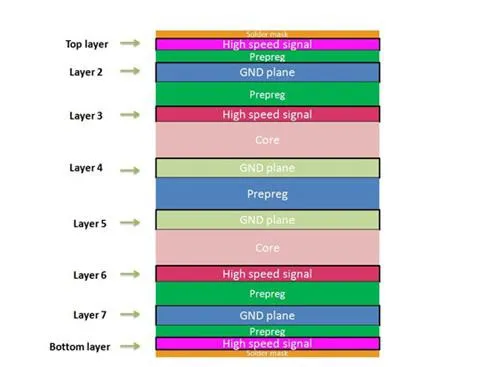
● Optimized Layer Stackup: Employ a symmetrical 8-layer PCB stackup configuration, placing power and ground planes in the central layers to minimize EMI. A typical and effective stackup might be Signal-Power-Ground-Signal-Signal-Ground-Power-Signal, which balances noise reduction with routing flexibility.
● Component Grouping and Loop Reduction: Group related input, output, and control components strategically to shorten critical current paths. For example, positioning input capacitors close to the converter IC stabilizes the input voltage, aiming for ripple below 100mV. Additionally, minimizing the area of high-frequency current loops, especially in switching converters, reduces radiated EMI and improves efficiency, particularly at frequencies above 1 MHz.
● Effective Shielding: Implement internal ground planes to shield sensitive analog signals from the noise generated by switching nodes. This ensures clean operation in mixed-signal designs, where high-frequency digital signals coexist with sensitive analog circuits.
Material Selection and Manufacturing for 8-Layer Power PCBs
The successful performance of an 8-layer PCB in power electronics is also heavily dependent on judicious material choices and precise manufacturing techniques.
Selecting High-Performance Materials
● High-Thermal Conductivity Materials: For high-current designs, opt for substrates with superior thermal conductivity, such as metal-core PCBs or enhanced FR-4 variations. Seek materials with a thermal conductivity exceeding 1 W/mK to effectively manage and dissipate heat.
● Appropriate Copper Weight: Utilize heavier copper weights (2-3 oz/ft²) for power layers. This is crucial for handling substantial currents without experiencing excessive resistance or undesirable heat generation.
Advanced Via Design and Manufacturing Accuracy
● Via Design: Incorporate buried and blind vias to connect internal layers. This strategy maximizes routing density without cluttering the surface layers. Ensure these vias are properly filled or plated to reliably handle high currents.
● Manufacturing Tolerances: Partner with a large PCB manufacturer capable of maintaining extremely tight tolerances for trace widths and spacing. This precision is especially critical for high-voltage designs, where even minor deviations can compromise safety and lead to catastrophic failure.
Overcoming Common Challenges in 8-Layer Power PCB Designs for Power Electronics
Designing an 8-layer PCB for high current and voltage applications presents several inherent challenges. Anticipating these issues and having pre-planned solutions is key to a successful design.
Addressing Signal Integrity and Thermal Hotspots
● Signal Integrity Issues: High-frequency switching often leads to crosstalk. To mitigate this, employ differential pair routing and position signal layers adjacent to solid ground planes to maintain precise impedance control. Aim for a characteristic impedance of 50 ohms for all critical signals.
● Thermal Hotspots: Uneven heat distribution can severely damage components and degrade performance. Utilize thermal simulation tools during the design phase to accurately identify and proactively mitigate potential hotspots before the manufacturing process begins.
Managing Cost Constraints
Multi-layer PCBs, especially those designed for high power, are inherently more expensive than simpler boards. To manage cost effectively without compromising performance, optimize the design by minimizing the total via count and, where feasible, utilizing standard, readily available materials.
Real-World Case Studies and Performance Data
The benefits of an 8-layer PCB become easier to understand when viewed through real-world use cases. While exact results depend on the application, several common patterns show why engineers choose this structure.
In a DC-DC power converter, placing the input capacitors close to the switching stage and dedicating internal planes to power and ground can reduce noise, improve transient response, and lower EMI. A well-planned stackup often produces cleaner waveforms than a simpler board because the return current path is more controlled.
In a power MOSFET layout, compact gate-drive routing and nearby decoupling can lower switching losses and reduce ringing. Adding thermal vias under the MOSFET pad improves heat removal, which helps maintain safe junction temperatures during continuous operation.
In an IGBT layout, stronger current paths and better isolation help support higher power levels. Because IGBTs often operate in demanding industrial systems, the combination of wide conductors, robust thermal spreading, and careful gate-drive separation is especially valuable.
In a high voltage PCB design, extra layers allow better physical separation between high-voltage and low-voltage sections. That can improve safety margin and reduce unwanted coupling. In many products, this is the difference between a design that merely functions and one that survives long-term use in the field.
These examples show a consistent theme: the advantage of an 8-layer PCB is not just the number of layers. It is the ability to distribute power, heat, and signal responsibility across the board in a controlled way.
Conclusion: Maximizing Power Electronics with 8-Layer PCBs
An 8-layer PCB offers unparalleled advantages for contemporary power electronics, particularly in applications demanding robust handling of high current and voltage. From meticulously optimizing trace widths in high-current designs to ensuring impeccable electrical isolation in high-voltage configurations, these multi-layered boards provide the essential flexibility and superior performance required for complex and critical applications. Whether you are developing an 8-layer PCB power MOSFET layout, an 8-layer PCB IGBT layout, or an 8-layer PCB power converter design, diligently adhering to best practices—including strategic layer allocation, comprehensive thermal management, and precise component placement—will consistently lead to superior and reliable results.
By effectively harnessing the advanced capabilities of multi-layer PCBs, engineers can construct power electronics systems that are not only highly efficient but also exceptionally reliable under the most demanding operational conditions. Through careful planning and an unwavering attention to detail, your designs can readily meet and exceed the rigorous demands of modern applications, spanning a wide array of sectors from sophisticated industrial systems to innovative renewable energy solutions.


