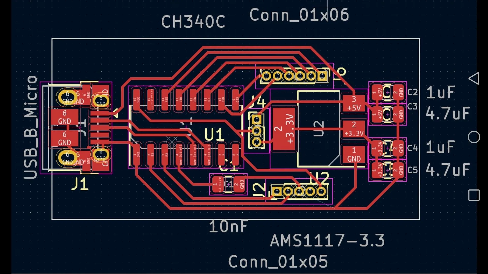
What is a USB PCB?
A USB PCB (Printed Circuit Board) refers to the specific physical layout and circuitry designed to support Universal Serial Bus (USB) communication protocols. It is the hardware foundation that houses the USB connector, the USB transceiver or controller Integrated Circuits (ICs), and the highly specific trace routing required to manage high-speed differential data pairs, power delivery (VBUS), and grounding.
Because USB has evolved from a simple peripheral connection into a high-speed, high-power interface (especially with the advent of USB-C and Power Delivery), a USB PCB is no longer just a simple wiring job. It requires meticulous high-speed digital and RF design principles to ensure data flows quickly, safely, and without interruption.
Why Thoughtful USB Interface Design is Crucial for Data Reliability
USB interfaces are ubiquitous, connecting everything from personal electronics to industrial systems and IoT devices. They serve as a universal conduit for data exchange, often at high speeds. However, a poorly conceived PCB design can lead to significant problems such as signal degradation, data corruption, or even system malfunctions. Issues like mismatched impedance or unwanted signal reflections can severely disrupt communication.
By meticulously addressing key design elements, including careful trace routing and appropriate connector selection, designers can preempt these common pitfalls. A focused approach ensures consistent and dependable performance for any USB application. This guide will delve into each critical aspect of USB PCB design, providing practical advice and specific recommendations for achieving successful outcomes.
What Are the Key USB PCB Design Requirements for Different USB Standards?
Before initiating your layout in your CAD software, it is essential to identify the specific USB standard your project will utilize. Each version comes with distinct demands regarding data transfer rates, routing complexity, and signal integrity.
To help you visualize the hardware requirements across different generations, here is a quick reference guide for USB PCB designers:
Table: USB Standards and PCB Design Requirements Comparison
| USB Standard | Max Data Rate | Active Data Pairs | Target Differential Impedance | Primary Connector(s) |
| USB 2.0 (High-Speed) | 480 Mbps | 1 Pair (D+ / D-) | 90 Ohms (±10%) | Type-A, Micro-B, USB-C |
| USB 3.2 Gen 1 (SuperSpeed) | 5 Gbps | 3 Pairs (1 Legacy, 2 TX/RX) | 90 Ohms (±10%) | Type-A, Type-B, USB-C |
| USB 3.2 Gen 2 (SuperSpeed+) | 10 Gbps | 3 Pairs (1 Legacy, 2 TX/RX) | 90 Ohms (±10%) | USB-C, Type-A |
| USB 4 / Thunderbolt 4 | 40 Gbps+ | Multiple High-Speed Lanes | 85 Ohms (±10%) | USB-C strictly |
-
USB 2.0 (High-Speed): Operating at up to 480 Mbps, USB 2.0 relies on a single differential pair (D+ and D-). The primary requirement here is precise impedance control, targeting a differential impedance of exactly 90 ohms (±10%).
-
USB 3.0 / 3.1 / 3.2 (SuperSpeed): These standards push data rates to 5 Gbps, 10 Gbps, or even 20 Gbps. In addition to the legacy D+/D- pair, they introduce multiple extra differential pairs for "SuperSpeed" transmit (TX) and receive (RX). At these gigahertz frequencies, you must enforce much stricter impedance tolerances, ultra-tight trace length matching, and rigorous via minimization to prevent signal loss.
-
USB Type-C & USB 4: USB-C is not a protocol, but a highly versatile connector standard that accommodates USB 2.0, USB 3.x, Thunderbolt, and USB Power Delivery (up to 240W). Its compact form factor, reversible plug orientation, and high pin density (24 pins) necessitate exceptionally precise routing. Note that for ultra-high-speed standards like USB 4 over Type-C, the target differential impedance for the high-speed TX/RX lanes often drops to 85 ohms to align with PCIe standards, requiring careful stackup adjustments.
Related Reading: Integrating USB-C into PCBs: Essential Design Practices
How Trace Impedance and Signal Reflections Impact Signal Integrity
Maintaining accurate trace impedance is arguably the most vital element in USB PCB design. Inconsistencies in impedance along the signal path generate signal reflections—where a portion of the transmitted energy bounces back toward the source. This causes data errors, jitter, and a reduction in transfer speeds.
To achieve the target 90-ohm differential impedance and minimize reflections, several strategies must be employed:
-
Trace Dimensions and Stackup: Utilize a PCB impedance calculator to precisely determine trace width and spacing. On a standard FR-4 board, an 8-mil trace width and 6-mil spacing might yield 90 ohms on a two-layer board, but for USB 3.0+, a minimum 4-layer stackup is required to route signals closely over a continuous, solid ground plane.
-
Material Selection: While standard FR-4 is sufficient for USB 2.0, high-speed USB 3.x designs often benefit from low-loss dielectric materials (like Rogers or Megtron) to minimize signal attenuation.
-
Smooth Trace Bends: Route traces with gradual, smooth curves or 45-degree angles. Sharp 90-degree corners create localized capacitance changes, resulting in instant impedance drops and harsh reflections.
-
Optimal Component Placement: Position the USB connector as close as physically possible to the USB controller IC. Shorter traces mean fewer opportunities for parasitic inductance and capacitance to degrade the signal.
USB Routing Guidelines: Best Practices for Differential Pair Routing and PCB Layout
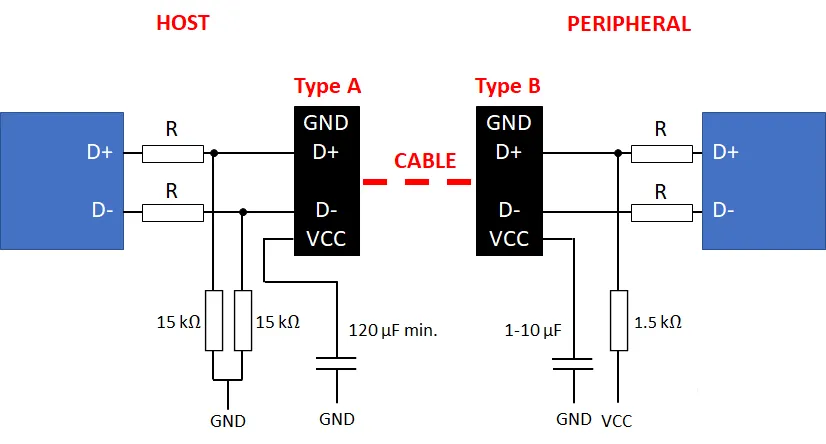
An expertly designed USB interface integrates differential routing rules with holistic board layout strategies. Because USB data lines (D+/D-, TX/RX) function as differential pairs, they transmit equal and opposite signals. Any imbalance between them translates to noise and data loss.
Guidelines for Differential Pairs:
-
Strict Length Matching: Strive to keep trace lengths identical. For USB 2.0, a variance of less than 150 mils is acceptable. For USB 3.0, aim for a discrepancy under 15 mils (or even 5 mils for 10 Gbps) to prevent timing skew.
-
Consistent Spacing (Coupling): Maintain a uniform distance between the two traces throughout their entire route to preserve the 90-ohm impedance. Do not split the pair around vias or components.
-
Via Minimization: Every via introduces an impedance discontinuity. Route USB pairs on a single layer (preferably the top or bottom) directly from the IC to the connector. If vias are unavoidable, use them symmetrically on both traces.
Related Reading: USB-C Integration on PCBs: A Design Guide for Engineers
Overall PCB Layout Guidelines:
-
Dedicated Planes: Allocate separate, stable layers for power (VBUS) and ground. A continuous ground plane beneath the USB traces provides a low-impedance return path and suppresses EMI.
-
Isolate from Noise: Keep USB traces strictly away from noisy digital circuits, switching regulators (SMPS), and clock generators to prevent cross-talk.
-
Decoupling: Place decoupling capacitors (e.g., 0.1 μF and 1 μF) immediately next to the power pins of the USB controller IC to filter out high-frequency noise.
Related Reading: Enhancing USB Performance: A Guide to Optimal PCB Layout and Signal Integrity
How Do I Select the Right USB Connector for My Design?
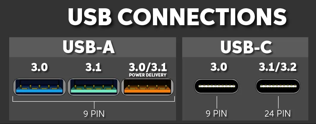
The choice of USB connector is as vital as the trace routing itself, influencing both the physical connection and the overall signal quality and durability of the interface. With numerous options available—such as Type-A, Type-B, Micro-USB, and USB-C—your selection should align with the specific application and the targeted USB standard.
Key Considerations for Connector Selection
When choosing a USB connector, keep the following factors in mind:
- USB Version Compatibility: Confirm that the connector fully supports the USB standard you intend to use. For instance, USB-C connectors are highly versatile for modern designs, offering support for USB 2.0, 3.0, and newer standards, along with reversible plug orientation.
- Physical Footprint: For devices with limited space, compact connectors like Micro-USB or USB-C are ideal. In industrial environments where robustness is key, sturdier options like Type-A or Type-B might be more appropriate.
- Durability Rating: Evaluate the connector's mating cycle rating, which indicates its expected lifespan under repeated insertions. USB-C connectors often boast ratings up to 10,000 cycles, making them highly durable for frequent use.
- Signal Pin Requirements: Higher-speed standards, such as USB 3.0, necessitate additional pins for their SuperSpeed data lines. Verify that the selected connector accommodates all the necessary signals for your specific design.
A thoughtfully chosen connector guarantees a reliable physical and electrical connection, significantly reducing the likelihood of data transfer problems.
Overcoming Common Challenges in USB PCB Design
Despite careful planning, designing USB PCBs can present various challenges. Anticipating these issues and having solutions ready can streamline the development process.
Addressing Common USB Design Hurdles
Here are some frequent problems encountered and practical ways to overcome them:
- EMI Interference: High-speed USB signals are susceptible to, and can generate, electromagnetic interference. Mitigate this by implementing effective shielding, ensuring proper grounding, and incorporating ferrite beads on power lines to filter noise.
- Space Constraints: In compact device designs, accommodating USB traces and connectors can be difficult. Prioritize short, direct routing paths and consider using smaller form-factor connectors like USB-C to conserve board space.
- Signal Skew: Mismatched trace lengths within differential pairs are a primary cause of signal skew. Utilize advanced PCB design software features that offer length-matching tools to ensure traces are kept as equal as possible.
Proactively tackling these challenges early in the design cycle can prevent costly revisions and delays in the project timeline.
Testing and Validating Your USB PCB Design for Reliability
Once your PCB is designed and manufactured, comprehensive testing is indispensable to confirm that it facilitates reliable data transfer. This validation phase ensures the design meets performance specifications and functions as intended in real-world scenarios.
Essential Methods for Design Validation
Employ these key testing methods to thoroughly evaluate your USB PCB design:
- Signal Integrity Analysis: Use a high-bandwidth oscilloscope to meticulously inspect the USB data lines for any signs of signal reflections, jitter, or unwanted noise. Crucially, verify that the eye diagram generated from the signals meets the specific requirements outlined in the USB specification for your chosen standard.
- Impedance Verification: Employ a time-domain reflectometer (TDR) to accurately measure the differential impedance of your traces. Confirm that these measurements precisely match your target impedance (e.g., 90 ohms for USB 2.0).
- Functional Compatibility Testing: Connect your developed device to a diverse range of USB hosts and peripheral devices. This helps confirm expected data transfer rates, ensures broad compatibility, and validates overall operational performance across various scenarios.
Rigorous testing helps identify and rectify potential issues before they reach end-users, ensuring the delivery of a high-quality, dependable product.
Crafting Reliable USB Interfaces Through Optimal PCB Design
Developing a PCB for USB interfaces demands meticulous attention to detail. This ranges from precisely controlling USB trace impedance and executing accurate differential pair routing to selecting appropriate connectors, minimizing signal reflections, and optimizing the overall USB PCB layout. By adhering to the comprehensive guidelines and best practices outlined in this guide, engineers can create designs that guarantee reliable data transfer across a multitude of applications.
Begin with a clear understanding of the specific USB standard relevant to your project. Then, shift your focus to rigorous impedance control, precise trace routing, and judicious component selection. With a well-conceived layout and thorough testing, your USB interface will consistently deliver robust performance, whether it’s integrated into a consumer gadget or a complex industrial system. At AIVON, we are dedicated to providing engineers with the high-quality PCB manufacturing and assembly capabilities required to bring these complex, high-speed USB designs to life successfully.
FAQs
Q1: Can I repair a broken battery charger PCB?
A1: While it is possible to replace a blown capacitor or a burnt resistor if you have soldering skills, it is generally not recommended to repair AC-to-DC wall chargers (like smartphone bricks). The high-voltage AC section poses a severe shock hazard, and improperly repaired safety components could cause electrical fires.
Q2: What is the difference between a Power Supply and a Battery Charger PCB?
A2: A power supply provides a constant, steady voltage (e.g., exactly 12V) regardless of what is plugged into it. A battery charger PCB is much smarter; it actively alters its voltage and current output based on the battery's specific state of charge, transitioning through different phases (like bulk charging and trickle charging) to safely fill the battery.
Q3: Why do some battery chargers make a high-pitched whining noise?
A3: This is known as "coil whine." Inside the battery charger PCB, magnetic components like transformers and inductors expand and contract microscopically as high-frequency electrical pulses pass through them. Sometimes, this physical vibration hits a resonant frequency that falls within the range of human hearing, producing a faint whine. It is generally harmless and does not indicate a failing charger.


