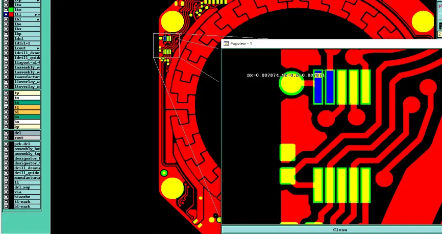
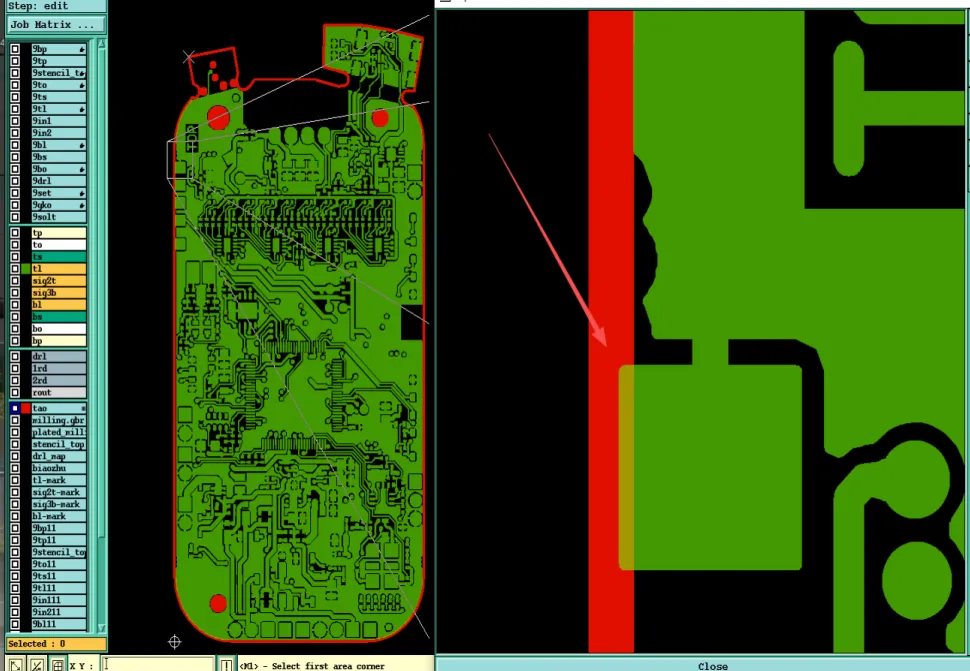
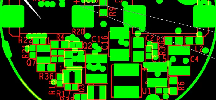
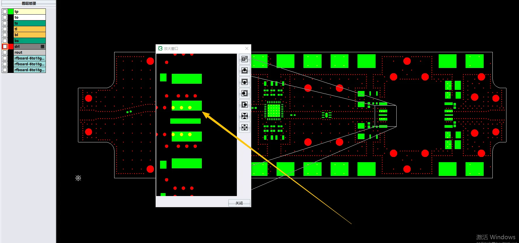
Coupons
Help
  • FAQ
    browse most common questions
  • Live Chat
    talk with our online service
  • Email
    contact your dedicated sales:
0

Engineering Cases

Engineering Cases focuses on real PCB engineering reviews, manufacturing challenges, and production optimization processes from actual fabrication projects. This category highlights how different PCB designs are evaluated and adjusted during engineering review, covering topics such as stack-up analysis, impedance control, drill optimization, copper balancing, solder mask alignment, DFM review, and production risk assessment across various PCB applications. The content in this section is based on practical manufacturing scenarios rather than theoretical introductions. Each engineering case demonstrates how specific PCB issues are identified, analyzed, and resolved during production preparation and fabrication. These records help engineers, purchasers, and hardware teams better understand the relationship between PCB design decisions and manufacturing stability, yield control, and process reliability. Topics may include multilayer PCB engineering review, HDI process optimization, flexible PCB manufacturing considerations, heavy copper processing adjustments, surface finish selection, Gerber data verification, and other real-world PCB production experiences. By organizing engineering challenges and process solutions into structured case content, this category provides valuable insight into practical PCB manufacturing and engineering workflow management.

 
2-Layer High-TG FR-4 PCB Engineering Case: Copper Thickness vs. Fine Line Conflict and Solder Mask Bridge Challenges in BGA Region
FR4 PCB Double-Sided PCB

2-Layer High-TG FR-4 PCB Engineering Case: Copper Thickness vs. Fine Line Conflict and Solder Mask Bridge Challenges in BGA Region

Senior PCB CAM engineer shares a real 2-layer FR-4 TG170 manufacturing case study. Discover critical DFM issues including 2oz copper thickness conflict with tight 6.89mil spacing and BGA solder mask bridge challenges at 7.87mil clearance. Learn how we resolved the issues through targeted EQs to prevent etching defects, solder bridging, and production scrap. Essential DFM insights for reliable PCB fabrication.

Engineering Case Study: 4-Layer 1.0mm FR-4 PCB Edge Clearance and Stamp Hole Spacing DFM Review
FR4 PCB 4-Layer PCB

Engineering Case Study: 4-Layer 1.0mm FR-4 PCB Edge Clearance and Stamp Hole Spacing DFM Review

Senior CAM engineer case study on a 4-layer 1.0mm FR-4 PCB. Discover critical DFM issues including insufficient copper-to-outline clearance causing exposed copper risks, tight stamp hole spacing, process edge copper pour recommendation, and 0.5mm hole clarification. Learn how our engineering team resolved these challenges to prevent edge defects, peeling, and depanelization problems. Practical insights for PCB designers.

8-Layer FR-4 PCB Engineering Case: Critical DFM Challenges in Copper Weight, Panelization, and Edge Clearance
FR4 PCB 8-Layer PCB

8-Layer FR-4 PCB Engineering Case: Critical DFM Challenges in Copper Weight, Panelization, and Edge Clearance

Senior PCB CAM engineer shares a real 8-layer FR-4 TG170 engineering case study. Discover critical DFM issues including inner layer 2oz copper vs 4mil spacing conflicts, panelization optimization, edge clearance problems, and solder mask inconsistencies. Learn practical manufacturing resolutions and key takeaways to avoid production delays and yield loss.

4-Layer 1.2mm FR-4 PCB CAM Engineering Case: Panelization, Stackup Adjustment, and Fiducial Protection Challenges
FR4 PCB 4-Layer PCB

4-Layer 1.2mm FR-4 PCB CAM Engineering Case: Panelization, Stackup Adjustment, and Fiducial Protection Challenges

Senior PCB CAM engineer analyzes a real 4-layer 1.2mm FR-4 PCB engineering case. Explore key DFM challenges including stackup adjustment with copper-clad cores, 3x3 panelization with V-cut + routing, stamp hole optimization, fiducial protection rings, UL marking conflicts, and silkscreen placement. Learn how our team resolved these manufacturing risks through targeted EQs to prevent depanelization failures, assembly misalignment, and quality issues. Practical insights for better PCB design.

Engineering Case Study: 2-Layer Rogers RO4350B High-Frequency PCB Edge Clearance and Via-on-Pad DFM Review
Rogers PCBs High-Frequency PCB

Engineering Case Study: 2-Layer Rogers RO4350B High-Frequency PCB Edge Clearance and Via-on-Pad DFM Review

Senior CAM engineer case study on a 2-layer 0.254mm Rogers RO4350B high-frequency PCB. Explore key DFM challenges including copper-to-outline edge clearance risks, via-in-pad resin plugging, no bottom solder mask yellowing acceptance, and slot size inconsistencies. Learn how our engineering team resolved these issues to ensure signal integrity, assembly reliability, and production success. Practical insights for RF PCB designers.

4-Layer FR-4 PCB Engineering Review Case: Stackup Deviation, Countersink Hole Depth, and Material Availability Challenges
FR4 PCB 4-Layer PCB PCB Design Review

4-Layer FR-4 PCB Engineering Review Case: Stackup Deviation, Countersink Hole Depth, and Material Availability Challenges

Senior PCB CAM engineer shares a real 4-layer FR-4 PCB engineering case study (H4P-2912-AI18148A). Discover key DFM issues including stackup thickness deviation, 1.35mm countersink hole processing on copper, core material availability challenges, and strict drill tolerances. Learn how our team resolved these manufacturing risks through EQ clarification to prevent warpage, plating defects, and production delays. Essential DFM insights for PCB designers.

6-Layer FR-4 PCB DFM Case Study: Resolving Panelization, Trace Compensation, and Edge Clearance Issues in Production Review
FR4 PCB 6-Layer PCB DFM Review

6-Layer FR-4 PCB DFM Case Study: Resolving Panelization, Trace Compensation, and Edge Clearance Issues in Production Review

Discover a real 6-layer FR-4 PCB engineering case study from a senior PCB CAM engineer. This detailed DFM review covers panelization mismatch, trace width compensation, hole-to-edge clearance, inner copper thickness confirmation, and other critical manufacturability issues. Learn why factories raise EQs, the production risks if ignored, and practical DFM insights to avoid delays and improve yield in multilayer PCB fabrication.

2-Layer Ultra-Thin FPC DFM Review: Large Panelization Challenges and Silkscreen Legibility Issues
Ultra-Thin PCB Double-Sided PCB DFM Review

2-Layer Ultra-Thin FPC DFM Review: Large Panelization Challenges and Silkscreen Legibility Issues

As a senior PCB CAM engineer, this real 2-layer 0.2mm ultra-thin FPC engineering case study reveals critical DFM problems with oversized 1x30 panelization, material shrinkage control, tooling hole limitations, and fine silkscreen legibility. Learn how we resolved the EQs by proposing a practical 14pcs panel layout and confirming character blurring acceptance to ensure manufacturability and SMT compatibility. Valuable insights for flexible PCB designers.

Engineering Case Study: 4-Layer FR-4 PCB Hole Spacing Optimization and Silkscreen Character Height DFM Review
4-Layer PCB FR4 PCB

Engineering Case Study: 4-Layer FR-4 PCB Hole Spacing Optimization and Silkscreen Character Height DFM Review

Senior CAM engineer case study on a 4-layer FR-4 PCB. Explore critical DFM issues including tight hole-to-hole spacing requiring diameter compensation, single-sided pad processing, and undersized silkscreen characters below minimum height. Learn how our engineering team resolved these manufacturing challenges to prevent drill breakout, poor legibility, and production defects. Practical insights for PCB designers.

Engineering Case Study: 4-Layer 0.4mm Thin FR-4 PCB Tight BGA Solder Mask Bridge and Marking DFM Review
FR4 PCB 4-Layer PCB

Engineering Case Study: 4-Layer 0.4mm Thin FR-4 PCB Tight BGA Solder Mask Bridge and Marking DFM Review

Senior CAM engineer case study on a 4-layer 0.4mm thin FR-4 PCB with blind vias. Explore critical DFM issues including tight BGA pitch preventing solder mask bridge, serial number & QR code marking confirmation, stencil vs solder mask mismatches, and stackup verification. Learn how our engineering team resolved these risks to prevent solder bridging, assembly failures, and production delays. Essential insights for high-density thin PCB designers.

Engineering Case Study: 2-Layer 0.2mm Ultra-Thin FPC DFM Review - Solder Mask Thickness and Panelization Challenges
Flexible PCB Double-Sided PCB

Engineering Case Study: 2-Layer 0.2mm Ultra-Thin FPC DFM Review - Solder Mask Thickness and Panelization Challenges

Senior CAM engineer case study on a 2-layer 0.2mm ultra-thin flexible PCB. Explore critical DFM challenges including white solder mask thickness conflict, no process edges on 20x1 panel, trace-to-outline clearance risks, and silkscreen character issues. Learn how our team resolved these manufacturing problems to prevent shorts, scattering, and yield loss. Practical insights for thin flex PCB designers.


2026 AIVON.COM All Rights Reserved
Intellectual Property Rights | Terms of Service | Privacy Policy | Refund Policy