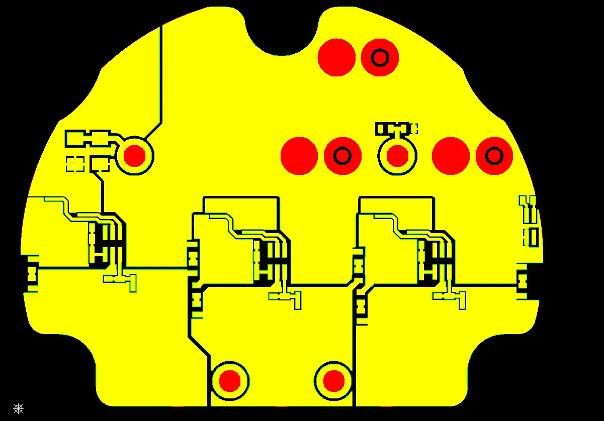
A 4-layer FR-4 board measuring 158.4 mm × 87.8 mm with 1.0 mm finished thickness and 1 oz copper on both outer and inner layers arrived for engineering review under factory number. The design used a customer-supplied 4×2 panel with V-cut plus routing separation and no process edge. Immersion gold surface finish at 1 µin and a 3-day lead time completed the basic parameters. From a DFM perspective, the absence of any process border immediately raised concern because traces and copper features approaching the board outline leave almost no margin for mechanical separation tolerances.
The primary DFM review focused on whether the design could enter production without creating edge-related defects, solderability problems, or long-term reliability risks. Several features required clarification before fabrication could proceed safely.
Why Trace to Board Edge Clearance Became the Dominant Risk
During CAM inspection, multiple traces and copper features were found closer to the board outline than the minimum clearances required for the chosen separation methods. For routed edges the minimum recommended clearance is 0.2 mm; for V-cut edges the minimum is 0.4 mm. These values are not arbitrary. They account for tool run-out, panel registration tolerance, and the physical width of the cutting path. When copper lies inside these zones, the risk of edge exposure, copper burrs, or incomplete separation rises sharply.
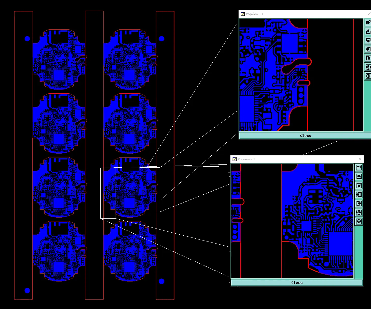
Figure 1: the circuit traces are too close to the board outline
The board ( #FR4-20260420-025 ) had zero process edge. That single design choice removed the usual buffer that protects outer copper during depaneling. Combined with a 4×2 customer panel and mixed V-cut plus routing, the clearance violations became the highest-priority manufacturability risk.
| Separation Method | Minimum Copper-to-Edge Clearance | Observed Condition | Risk Level |
|---|---|---|---|
| Routing | ≥ 0.2 mm | Multiple traces inside limit | High |
| V-cut | ≥ 0.4 mm | Copper features inside limit | High |
| Process edge | None present | 0 mm border | Elevated overall risk |
From a DFM perspective, the primary concern was manufacturing stability during depaneling. Without adequate clearance, the V-blade or router bit can contact copper, producing exposed edges, copper peeling, or micro-cracks that later become reliability failures.
Secondary Risks: Silkscreen on Pads and Open-Window IC Pads
Several silkscreen characters overlapped solder pads. Legend ink on a pad surface interferes with solder wetting and can create voids or incomplete joints during assembly. The DFM recommendation was to remove the overlapping text from the pads so that the solderable area remained clean. This is a standard preventive action under IPC-A-600 acceptability criteria for solderable surfaces.
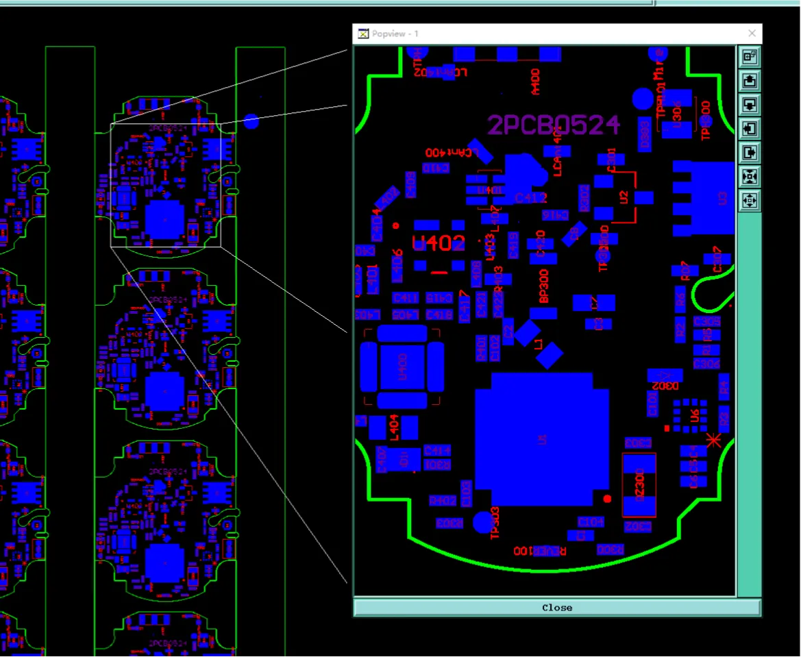
Figure 2: many characters designed on the pads
In addition, certain IC pads were designed with connected open windows in the solder mask. The original intent appeared to be continuous copper exposure across multiple pads. Fabricating exactly as drawn is possible, yet the configuration increases the chance of solder bridging between adjacent pins if the solder paste volume is not tightly controlled. The engineering team flagged the feature for customer confirmation rather than automatically altering the design.
A model number appeared on both the solder mask layer and the silkscreen layer. Dual placement is usually intentional for visibility after assembly, but it required verification that the mask-layer version would not create unwanted openings or cosmetic issues. Finally, an arrow-marked feature needed confirmation as a 1.5 mm MARK point so that optical alignment during assembly would remain reliable.
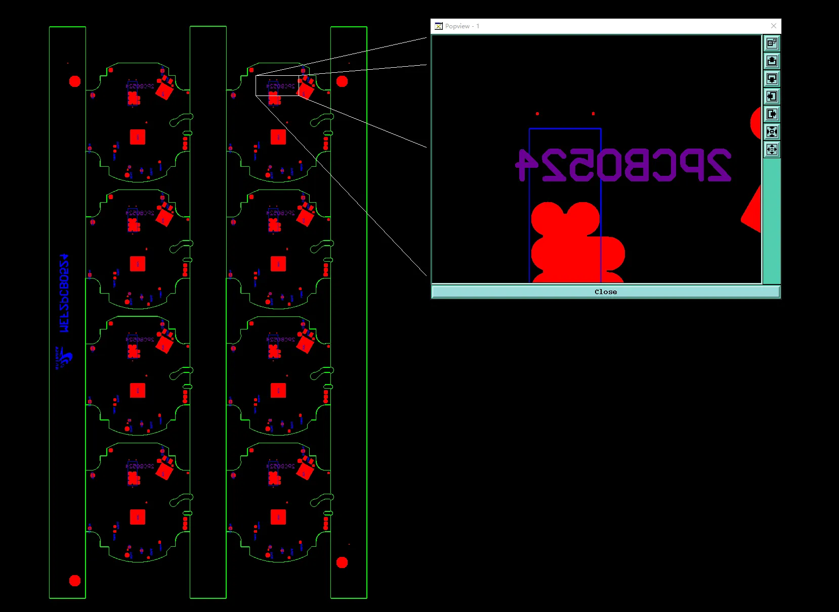
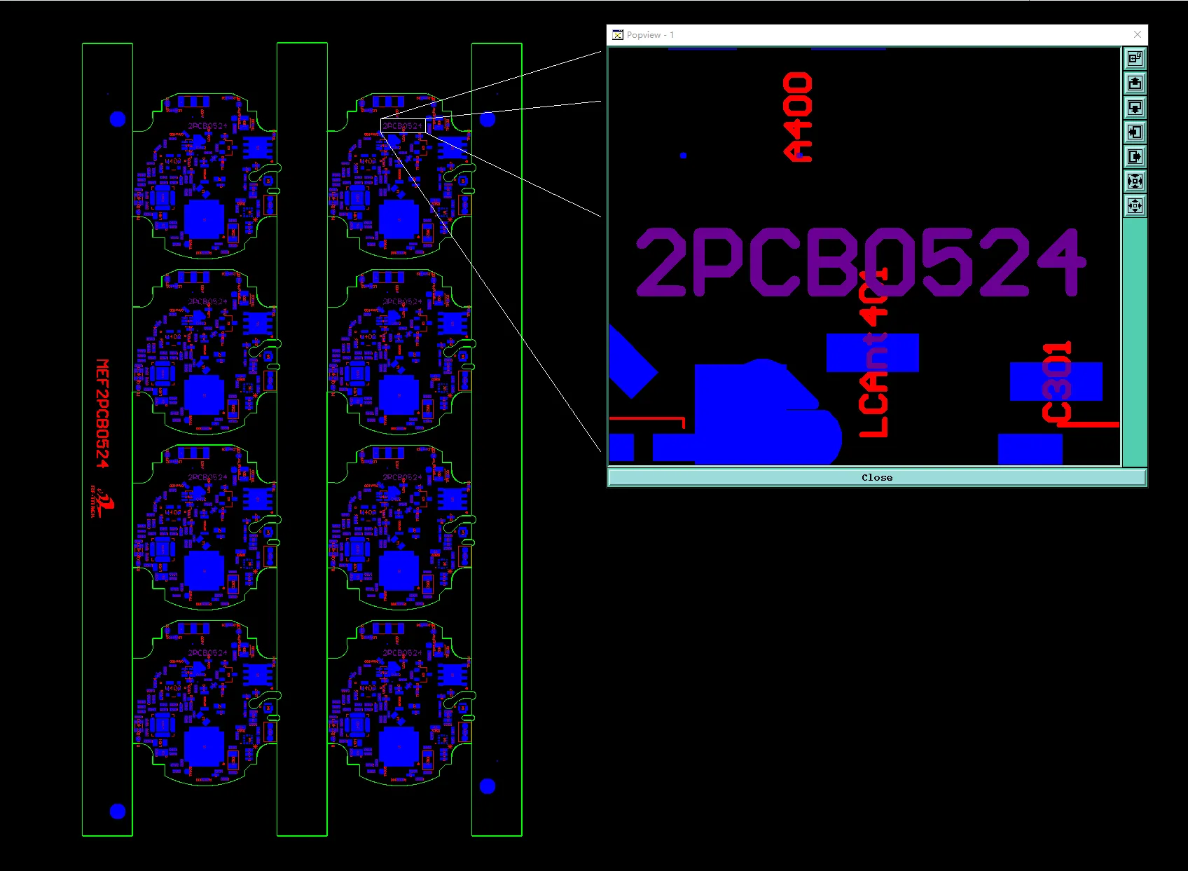
Figure 3, 4: model number appeared on both the solder mask layer and the silkscreen layer
How These Risks Could Affect Yield and Reliability
If the insufficient trace-to-edge clearances had been ignored, several realistic failure modes could appear:
- Copper exposure or burrs along the routed or V-cut edge, leading to short-circuit risk during handling or assembly.
- Localized copper peeling or delamination at the board perimeter under thermal or mechanical stress.
- Incomplete board separation, producing irregular edges that interfere with fixture seating or enclosure fit.
- Reduced dielectric strength at the edge, increasing the chance of surface tracking in humid environments.
According to common IPC-2221 spacing guidance and IPC-A-600 edge-condition criteria, copper features that fall inside the mechanical separation zone are considered high-risk for both yield and long-term reliability. On a 1.0 mm board the mechanical stresses during V-scoring and routing are concentrated near the surface; any copper lying within the cut path amplifies those stresses.
Silkscreen on pads would have produced soldering defects—voids, poor wetting, or tombstoning—directly reducing assembly yield. Open-window IC pads, if left unconfirmed, could have generated solder bridges that require rework or cause functional failures after reflow.
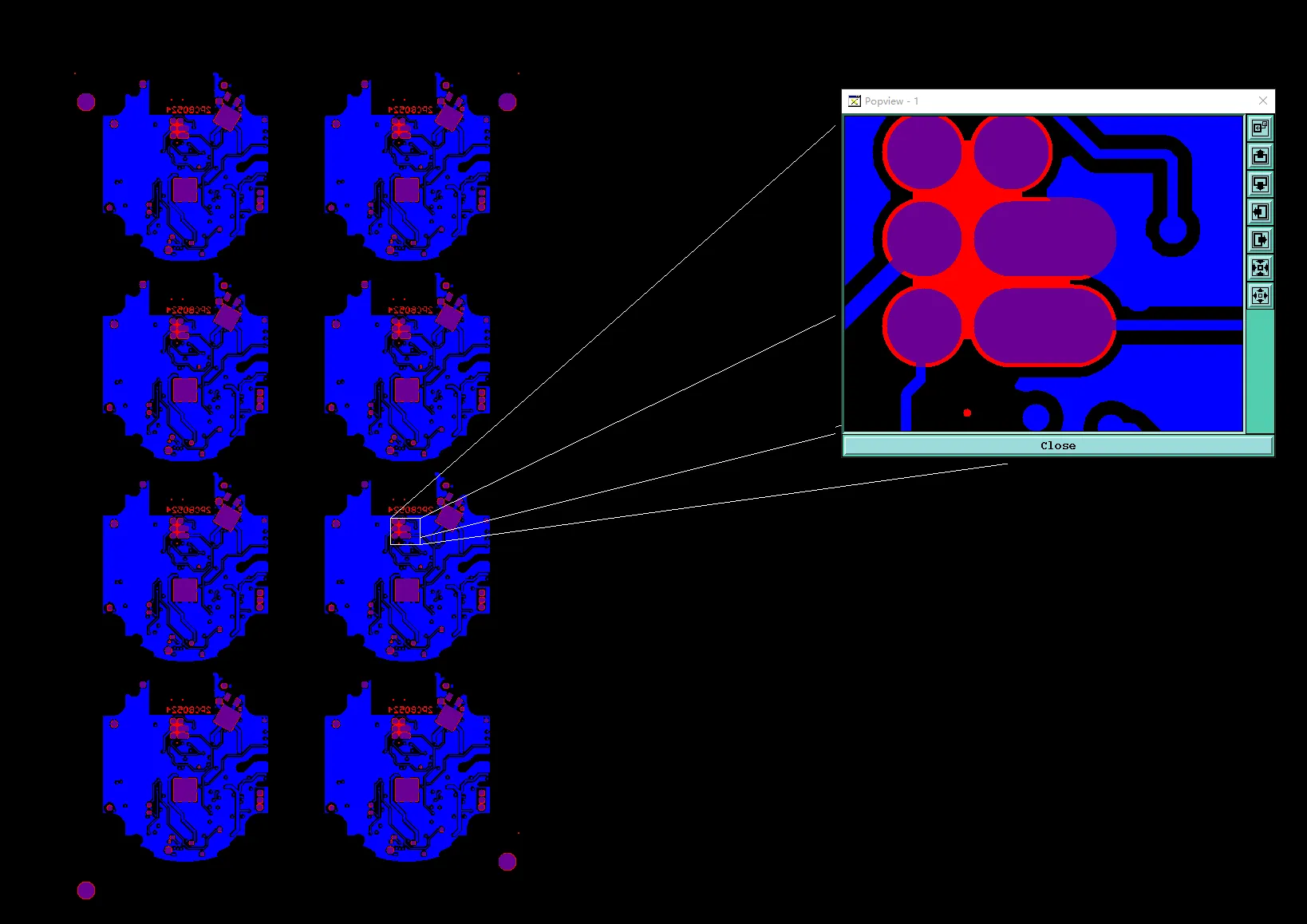
Figure 5: open-window IC pads
| Risk Feature | Potential Failure Mode | Impact on Yield | Impact on Reliability |
|---|---|---|---|
| Trace-to-edge clearance | Edge copper exposure, burrs, peeling | Scrap or rework at depaneling | Edge delamination, tracking |
| Silkscreen on pads | Poor wetting, solder voids | Assembly defects | Intermittent joints |
| Open-window IC pads | Solder bridging | Functional failures | Short circuits in field |
Failure Scenarios the Engineering Team Wanted to Prevent
Had production continued without clarification, the most probable sequence would have been as follows. During V-scoring the blade would have contacted copper that lay inside the 0.4 mm zone, generating copper debris and irregular edge geometry. Subsequent routing of the remaining outline would have further exposed copper along the board perimeter. Boards reaching assembly would have shown solder defects where silkscreen remained on pads. Any open-window IC sites would have been susceptible to bridging under standard paste volumes. The combined result would have been elevated scrap at depaneling, increased rework at assembly, and a higher probability of field returns caused by edge-related reliability issues.
These outcomes are preventable. The DFM review therefore treated every clearance violation and every pad-legend conflict as a risk that could be eliminated before the first panel was processed.
Preventive Actions Recommended by the DFM Team
The engineering team issued a clear set of preventive recommendations:
- Move all copper features a minimum of 0.2 mm from routed edges and 0.4 mm from V-cut edges. Where the difference was only 0.1 mm, a side-by-side comparison was provided so the customer could evaluate the visual and electrical impact of the small shift.
- Remove silkscreen characters that overlapped solder pads to restore full solderable area and eliminate wetting interference.
- Confirm whether the connected open-window design on IC pads was intentional; if so, proceed as drawn with awareness of bridging risk; if not, restore individual mask openings.
- Verify that the dual-layer model number placement was required and that the marked 1.5 mm feature was indeed a MARK point for optical alignment.
The customer reviewed the comparison drawings and accepted the outward movement of the V-cut and outline lines. The remaining items were confirmed or corrected in the same exchange. With these adjustments locked, the design entered production under controlled edge clearances and clean pad surfaces.
The small dimensional change did not alter electrical performance yet removed the primary source of edge-related defects. Silkscreen cleanup prevented a class of assembly defects that would otherwise have appeared only after reflow. Together the actions converted a set of latent risks into a stable manufacturing process.
Building Trust Through Proactive DFM
This case illustrates how a focused DFM review protects both yield and long-term reliability. Trace-to-board-edge clearance violations, silkscreen on pads, and ambiguous open-window features are common in customer-supplied panels that lack process borders. Each condition is easy to overlook in design software yet carries measurable production and field consequences. By raising the issues before any panel was fabricated, the engineering team eliminated the need for later scrap, rework, or reliability investigations.
Designers who engage early DFM review gain a practical advantage: the opportunity to adjust clearances, legend placement, and mask openings while the cost of change is still zero. The same preventive mindset applied to every subsequent design reduces the probability that similar edge or solderability risks will reappear.
FAQ
Q1: Why is a minimum 0.2 mm clearance required between copper and a routed board edge?
A1: Routing tools have run-out and the panel has registration tolerance. Copper closer than 0.2 mm can be contacted by the router bit, producing exposed copper, burrs, or peeling. Maintaining the clearance keeps the cut path clear of conductive material and protects edge integrity.
Q2: Why does V-cut require a larger 0.4 mm copper-to-edge clearance?
A2: A V-score blade removes material from both sides of the panel and creates a stress concentration line. Copper inside the 0.4 mm zone is more likely to be fractured or exposed during scoring and subsequent break-out, increasing the risk of edge defects and reduced dielectric strength.
Q3: What happens if silkscreen characters remain on solder pads?
A3: Legend ink prevents proper solder wetting. The result is voids, incomplete fillets, or weak joints that lower assembly yield and can become intermittent connections over time. Removing the overlapping text restores a clean solderable surface.
Q4: Are connected open-window IC pads always a problem?
A4: Not always, but they increase the probability of solder bridging between adjacent pins if paste volume is not tightly controlled. Confirmation that the design is intentional allows the process to proceed with awareness of the bridging risk; otherwise individual mask openings are preferred.
Q5: How does the absence of a process edge increase DFM risk?
A5: A process edge provides a sacrificial border that absorbs tool run-out and registration error. Without it, every copper feature near the outline is exposed to the full mechanical tolerance of the depaneling process, raising the chance of edge defects.
Q6: Why should designers confirm MARK-point size and location during DFM review?
A6: Optical alignment systems rely on accurately sized and positioned fiducials. An ambiguous or incorrectly sized MARK point can cause placement offset, leading to solder defects or open circuits that appear only after assembly.