-
 00:55
00:55
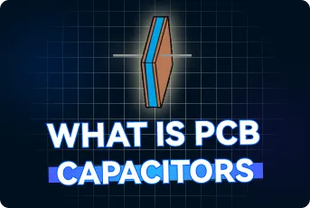
What Does a Capacitor Actually Do?
Capacitors are essential components in modern PCB design, responsible for energy storage, noise filtering, and stabilizing power delivery across electronic systems. This video explains how capacitors function at a fundamental level, including their structure of conductive plates separated by a dielectric material, and how different types are used in SMT assembly. It compares MLCC capacitors, which are ideal for high-frequency decoupling near ICs, with electrolytic capacitors that provide bulk energy storage and power stability. The video also highlights key design principles such as polarity awareness and the importance of placing decoupling capacitors close to active components. Understanding these concepts helps engineers improve signal integrity, reduce EMI, and enhance reliability in automotive, medical, industrial, and other high-performance PCB applications.
-
 00:51
00:51
Why Are PCB Vias Plugged?
Via plugging is an important PCB fabrication process that improves assembly quality, surface flatness, and long-term board reliability by filling plated vias with solder mask ink or epoxy. This video explains how via plugging prevents solder wicking, enhances SMT assembly, and supports high-density PCB designs. It also covers key manufacturing considerations, including proper via sizing, fill quality, curing processes, and inspection for defects such as voids or incomplete filling. In addition, the video discusses advanced techniques such as epoxy-filled and copper-capped via-in-pad structures used in HDI and multilayer PCBs. Understanding these practices helps engineers improve manufacturability, thermal performance, and reliability in automotive, medical, industrial, and other high-performance electronic applications.
-
 00:51
00:51
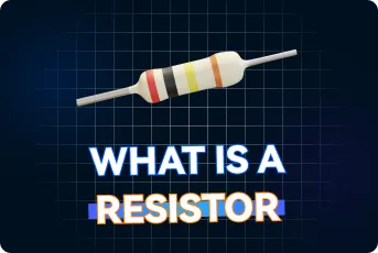
What Does a Resistor Actually Do in PCBs? SMD vs Through-Hole Explained
Resistors are fundamental electronic components that regulate current flow, protect sensitive devices, and ensure stable circuit operation. This video explains how resistors work by converting electrical energy into heat through controlled resistance and explores the factors that determine their resistance values. It also traces the evolution from traditional through-hole resistors to compact SMD components that support high-density PCB designs. In addition, the video highlights key considerations for resistor selection, including power rating, thermal management, and reliability. Understanding these principles helps engineers optimize circuit performance, improve manufacturing quality, and enhance the durability of rigid, HDI, and rigid-flex PCB applications.
-
 00:52
00:52
This PCB Hole Works without Solder | Press-fit Holes Explained
PCB press-fit holes are a solderless interconnection method used to create highly reliable electrical and mechanical connections between connectors and plated through-holes. This video explains how compliant pins are mechanically inserted into precisely manufactured holes, forming a gas-tight connection through controlled compression and spring-back against the plated barrel. It highlights key design requirements such as accurate hole sizing, strong copper plating, adequate annular rings, and strict manufacturing tolerances. The video also discusses common design risks, including insufficient contact force or barrel damage caused by incorrect hole dimensions. These guidelines are essential for ensuring robust performance in automotive, aerospace, industrial, and other high-reliability PCB applications during both prototyping and mass production.
-
 00:51
00:51
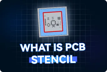
Your Soldering Problem May Start Here | PCB Stencil Selection Explained
PCB stencils play a crucial role in SMT assembly by controlling the precise amount of solder paste deposited onto component pads. This video explains how improper stencil selection can lead to defects such as solder bridging, weak joints, and open connections. It compares common stencil types, including laser-cut, electropolished, and step stencils, and discusses how stencil thickness influences paste volume, assembly quality, and first-pass yield. By understanding stencil design and selection principles, engineers can optimize solder paste printing, improve assembly reliability, and achieve better manufacturing results for HDI, consumer, medical, automotive, and other high-density PCB applications.
- Products & Service
- Company
- About AIVON
- Contact
- News
- Blog
- Certification
-


- Payment
-


2026 AIVON.COM All Rights Reserved