Introduction
Automotive electronics have advanced rapidly, driven by electrification, autonomous driving systems, and enhanced connectivity. Printed circuit boards (PCBs) in these applications must withstand extreme temperatures, vibrations, electromagnetic interference, and high power densities. Basic PCB design suffices for simpler components, but automotive PCB advanced design demands sophisticated techniques to ensure signal integrity, thermal management, and long-term reliability. Key methods include controlled impedance, embedded passives, back drilling, via stitching, and thermal plane design. These approaches address the unique challenges of vehicles, where failure can have severe safety implications. Mastering them allows engineers to optimize performance while meeting stringent reliability requirements.
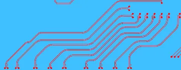
Controlled impedance forms the foundation of automotive PCB advanced design for high-speed signals found in advanced driver-assistance systems (ADAS), infotainment, and vehicle-to-everything (V2X) communication. Impedance mismatches lead to reflections, crosstalk, and data errors, which are unacceptable in safety-critical applications. Engineers achieve controlled impedance by precisely designing trace widths, spacing, and layer stackups, considering the dielectric constant of materials and copper thickness. The characteristic impedance depends on the geometry of the transmission line and the surrounding dielectric properties. For differential pairs common in automotive Ethernet or CAN-FD buses, symmetric routing maintains consistent impedance across the pair. Proper simulation and verification during design prevent issues that could degrade system performance under real-world conditions like temperature variations.
In multilayer boards, reference planes play a critical role in stabilizing impedance. Ground or power planes adjacent to signal layers provide return paths and reduce radiation. Automotive environments introduce challenges such as humidity and thermal cycling, which can alter dielectric properties and shift impedance values. Designers must select materials with low coefficient of thermal expansion and stable permittivity to minimize these effects. Testing involves time-domain reflectometry to measure impedance profiles along traces. Adhering to IPC standards for workmanship ensures consistency from design to fabrication.
Embedded Passives: Integrating Components for Compact, High-Performance Designs
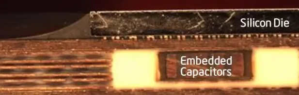
Embedded passives represent a leap in automotive PCB advanced design by integrating resistors, capacitors, and inductors directly into the board layers rather than as discrete surface-mount devices. This technique reduces board real estate, lowers parasitic inductance, and improves reliability by eliminating solder joints prone to fatigue in vibrating environments. Fabrication involves depositing resistive or capacitive materials between dielectric layers, patterned via photoimaging or laser trimming for precise values. Capacitors form from parallel plates separated by a high-k dielectric, while resistors use thin-film nickel-phosphorus alloys. In power electronics for electric vehicles, embedded passives handle decoupling needs close to ICs, minimizing loop inductance.
The process requires careful material selection to match the thermal expansion of surrounding layers, preventing delamination during reflow or operation. Automotive qualification demands assessment of drift under bias, temperature, and humidity, as per JEDEC guidelines for component reliability. Designers must model the embedded elements in simulations to predict frequency response and ensure they meet circuit requirements. This approach suits high-density modules like battery management systems, where space constraints are acute. Overall, embedded passives enhance electrical performance while simplifying assembly flows.
Challenges include variability in embedded component tolerances, often higher than discretes, necessitating design margins. Integration demands collaboration between PCB fabricators and designers early in the process. Post-fabrication testing verifies values using impedance analyzers or network analyzers. When implemented correctly, embedded passives contribute to smaller, lighter boards ideal for automotive weight reduction goals.
Back Drilling: Eliminating Via Stubs for High-Frequency Performance
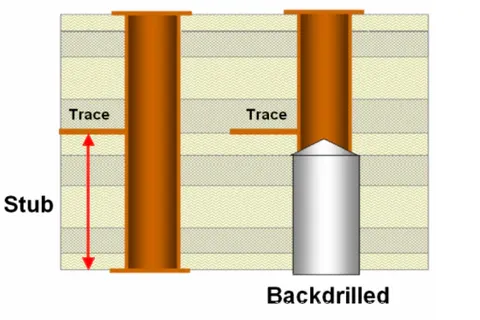
Back drilling removes unused via stub lengths in multilayer PCBs, a critical technique in automotive PCB advanced design for signals exceeding 1 GHz, such as in radar or LiDAR interfaces. Standard through-hole vias create capacitive and inductive stubs that cause signal reflections and insertion loss at high frequencies. The back drilling process uses a larger-diameter drill from the opposite side to excise the stub while leaving the barrel intact for interconnection. Optimal stub removal targets lengths below one-tenth of the signal wavelength to minimize return loss. Engineers specify back drill depths and shoulder control during design to ensure mechanical integrity.
In automotive applications, where boards stack multiple high-speed layers, back drilling preserves eye diagram quality and bit error rates. It also reduces crosstalk between adjacent vias. Fabrication tolerances for depth control are tight, typically within 0.1 mm, to avoid over-drilling into active sections. Designers incorporate back-drilled vias in stackups with blind or buried alternatives where possible, balancing cost and performance. Verification involves cross-section analysis and high-frequency S-parameter measurements.
Thermal stresses from automotive soldering and operation can affect via reliability post-back drilling, requiring robust plating. IPC guidelines outline acceptability criteria for via geometry and plating continuity. This technique proves essential for evolving standards in vehicle networking.
Via Stitching: Enhancing Current Handling and EMI Shielding
Via stitching connects multiple ground or power planes, distributing current evenly and providing low-impedance paths in automotive PCB advanced design. In high-current paths for motor drives or LED lighting, unstitched planes risk hot spots and voltage drops. Stitching vias, placed at intervals along traces, act as parallel conductors, reducing resistance and inductance. For EMI suppression, dense stitching around high-speed traces forms a Faraday cage effect, containing fields. Optimal spacing follows rules like via pitch less than one-twentieth of the wavelength or 1/10 of trace width.
Automotive power distribution networks benefit from stitched planes to handle peak currents without electromigration. In multilayer designs, stitching also equalizes potentials across planes split by clearance areas. Engineers calculate via count based on current density limits, typically 0.5-1 A per via depending on plating. Placement avoids signal vias to prevent coupling. Simulation tools model thermal rise and voltage gradients.
Maintenance of stitching integrity during thermal cycling demands robust design, aligning with J-STD standards for soldering reliability.
Thermal Plane Design: Managing Heat in Power-Dense Automotive Systems
Thermal plane design incorporates dedicated copper pours or embedded heat spreaders to dissipate heat from power components in electric vehicles and powertrains. High-power devices like IGBTs and MOSFETs generate significant joule heating, risking thermal runaway if unmanaged. Thick copper planes, often 2-4 oz/ft2, conduct heat laterally to vias or edges, coupled with thermal vias under hotspots. Designers optimize plane thickness, cutouts, and connectivity to balance electrical and thermal performance. In multilayer boards, buried planes serve as heat sinks, isolated from signals.
Automotive thermal profiles span -40°C to 150°C, necessitating materials with high glass transition temperatures. Via thermal resistance calculations guide array density, with filled vias preferred for better conductivity. Integration with chassis heatsinks via mechanical interfaces enhances overall cooling. Finite element analysis predicts junction temperatures under load cycles.
IPC specifications for conductor thickness and quality ensure manufacturability. This design mitigates hotspots, extending component life.
Best Practices for Integrating Advanced Techniques
Successful automotive PCB advanced design integrates these techniques holistically. Start with stackup optimization, balancing impedance, thermal, and mechanical needs. Simulate signal integrity, power delivery, and thermals iteratively. Collaborate with fabricators for DFM checks on back drilling and embedding. Prototype testing under accelerated life conditions validates designs. Document tolerances and processes for repeatability.
Layer budgeting prioritizes high-speed signals inner, power outer where possible. Material selection favors low-loss dielectrics for RF paths. Cost-benefit analysis weighs advanced features against volume production.
Conclusion
Advanced automotive PCB design techniques like controlled impedance, embedded passives, back drilling, via stitching, and thermal plane design elevate reliability and performance beyond basic layouts. They address the demanding requirements of modern vehicles, from high-speed data to power management. Engineers applying these methods systematically ensure compliance with industry benchmarks and superior field performance. As automotive electronics advance, proficiency in these areas remains essential for innovation and safety.
FAQs
Q1: What role does controlled impedance play in automotive PCB advanced design?
A1: Controlled impedance maintains signal quality in high-speed automotive interfaces like ADAS Ethernet by preventing reflections through precise trace geometry and stackup design. It counters environmental factors such as temperature swings that alter dielectric properties. Engineers verify it via TDR measurements, ensuring low bit error rates. This technique aligns with reliability standards for safety-critical systems.
Q2: How does back drilling improve high-frequency performance in automotive PCBs?
A2: Back drilling eliminates via stubs that cause signal loss and reflections in multilayer automotive boards used for radar or V2X. By removing excess barrel length, it preserves insertion loss margins at multi-GHz frequencies. Precise depth control during fabrication is key to integrity. This enhances overall system eye patterns and reduces crosstalk.
Q3: Why use via stitching in thermal plane design for automotive applications?
A3: Via stitching in thermal planes distributes heat and current evenly across layers in power-heavy automotive modules like inverters. It lowers thermal resistance through parallel paths and aids EMI containment. Proper spacing prevents hotspots, extending device lifetimes under cycling. Design rules base density on current and frequency needs.
Q4: What are the benefits of embedded passives in automotive PCB advanced design?
A4: Embedded passives save space, reduce parasitics, and boost reliability by avoiding solder joints in vibration-prone vehicles. Integrated into layers, they provide decoupling near ICs for stable power delivery. Tolerance management and material matching ensure performance. Ideal for compact battery or ECU boards.
References
IPC-6012E — Qualification and Performance Specification for Rigid Printed Boards. IPC, 2017
JEDEC J-STD-020E — Moisture/Reflow Sensitivity Classification. JEDEC, 2014
J-STD-001H — Requirements for Soldered Electrical and Electronic Assemblies. IPC, 2018


