Introduction
Smartwatches have transformed into multifunctional devices that demand seamless wireless connectivity for features like notifications, fitness tracking, and health monitoring. Central to this capability is the antenna integrated into the smart watch PCB design, which handles signals for Bluetooth, Wi-Fi, and other protocols in an extremely compact form factor. Electrical engineers face unique challenges in balancing antenna performance with the constraints of small PCB sizes, proximity to the human body, and interference from components like batteries and displays. Effective smart watch PCB antenna design ensures reliable data transmission, optimal power efficiency, and minimal signal loss. This article explores the principles, strategies, and best practices for antenna integration, focusing on placement, impedance matching, and protocol-specific considerations. By adhering to established engineering approaches, designers can achieve robust performance in wearable applications.
The Critical Role of Antennas in Smartwatch Connectivity
Antennas serve as the interface between the smartwatch's PCB electronics and the external wireless environment, converting electrical signals into electromagnetic waves and vice versa. In smartwatches, where PCB real estate is limited to mere square centimeters, poor antenna design can lead to reduced range, intermittent connections, and higher power consumption, draining the battery faster. The relevance intensifies with the rise of always-on connectivity for real-time syncing with smartphones or cloud services. Engineers must consider frequency bands like 2.4 GHz for Bluetooth and Wi-Fi, where wavelength fractions dictate minimum sizes, yet practical designs require miniaturization techniques. Body proximity introduces detuning due to tissue absorption, altering impedance and radiation patterns. Ultimately, well-designed antennas uphold the device's usability, making them a cornerstone of smart watch PCB antenna design.
Fundamentals of Antenna Types in Smart Watch PCBs
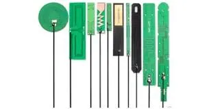
Smart watch PCB antenna design commonly employs planar structures suited to flat, multilayer boards, such as inverted-F antennas (IFA), meandered inverted-F antennas (MIFA), planar inverted-F antennas (PIFA), and chip antennas. IFA and MIFA configurations fold the radiating element to fit compact footprints while maintaining resonance at target frequencies. Chip antennas offer pre-tuned solutions for ultra-small spaces but demand precise keep-out zones to avoid performance degradation. These types operate on principles of quarter-wavelength resonance adjusted for the PCB's dielectric constant, typically around 4.5 for standard materials. Radiation patterns aim for omnidirectionality to support varied wrist orientations during use. Selection depends on board size, with PCB traces preferred for cost and integration when space allows.
Layer stackup influences efficiency, as ground planes act as reflectors shaping the pattern. Top-layer placement isolates the antenna from digital noise below. Low-loss dielectrics minimize signal attenuation, though standard substrates suffice for low-power protocols. Simulation verifies resonance and bandwidth before prototyping. Integration requires isolating RF sections from baseband circuitry to prevent coupling.
Optimizing Antenna Placement in Compact PCBs
Antenna placement profoundly impacts radiation efficiency and pattern in smart watch PCB antenna design, with edge or corner positions providing the clearest path for wave propagation. Positioning the antenna away from the PCB center maximizes clearance in multiple directions, reducing blockage by components or the user's body. Keep-out zones, free of copper, traces, and vias on all layers, extend around the radiating element to preserve field integrity. Ground planes should terminate smoothly before this zone, avoiding slots that distort currents. Proximity to batteries, metal frames, or displays causes detuning through capacitive coupling or shielding effects.
For wearables, orient the antenna to radiate away from the skin, as human tissue absorbs energy and shifts resonance lower. Mechanical enclosures must allow sufficient air gap, tested in final assembly. Multiple antennas for diversity require orthogonal polarization and spacing to minimize mutual coupling. Following IPC-2221 guidelines for high-frequency layouts ensures controlled environments around RF sections. Empirical tuning accounts for assembly variations.
Antenna Impedance Matching Techniques
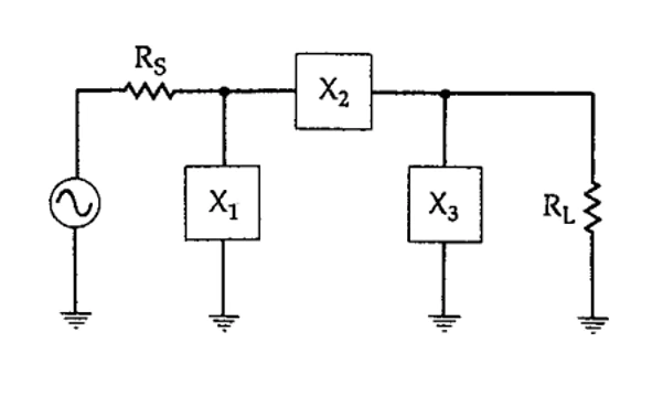
Impedance matching aligns the antenna's input impedance with the transceiver's 50-ohm output, maximizing power transfer and minimizing reflections quantified by voltage standing wave ratio (VSWR). Mismatch leads to return loss, reducing efficiency and range in smart watch PCB antenna design. Pi-networks or L-networks, using series inductors and shunt capacitors, provide tunability post-fabrication. Engineers measure complex impedance across the band with network analyzers, then compute component values for conjugate matching. Compact designs exhibit reactive components due to short lengths, necessitating compensation.
Feed lines employ microstrip or coplanar waveguide for consistent 50-ohm characteristic impedance, calculated from trace width, height, and dielectric. Vias near the feed connect to ground without encroaching on the keep-out. ESD protection diodes shunt transients without degrading matching. Bandwidth targets cover protocol channels, typically 80-100 MHz for Bluetooth. Iteration refines the network, validating S11 below -10 dB.
Bluetooth Antenna Design Considerations
Bluetooth antenna design in smartwatches prioritizes low-power operation at 2.4 GHz ISM band, favoring MIFA or chip types for their balance of size and efficiency. PCB traces integrate seamlessly, with meandering shortening the element while preserving quarter-wave resonance. Placement on the outer edge directs radiation outward, countering wrist absorption. Matching networks tune for the full BLE channel span, ensuring robust links up to several meters. Ground plane size stabilizes patterns, though miniaturization trades gain for compactness.
Body loading detunes resonance downward, addressed by overcompensating in free-space design. Diversity antennas improve reliability in obstructed scenarios. IPC-2228 provides sectional guidance for high-frequency boards, emphasizing RF-specific conductor rules. Prototyping verifies real-world performance with spectrum analyzers.
Wi-Fi Antenna Design Challenges
Wi-Fi antenna design introduces dual-band complexity (2.4/5 GHz) in the same compact footprint, stretching smart watch PCB antenna design limits. Multiband structures like slotted PIFA or stacked elements achieve coverage, but efficiency drops at higher frequencies due to smaller wavelengths. Placement mirrors Bluetooth, with added clearance for wider bandwidths. Matching requires broadband networks, often stepped-impedance lines alongside lumped elements. Higher path loss demands better gain, challenging low-profile constraints.
Enclosure and body effects exacerbate pattern nulls at 5 GHz, where penetration is poorer. Shared ground planes with Bluetooth necessitate isolation. Simulation models full stackup for accurate prediction. Practical validation includes throughput tests in operational bands.
Best Practices and Common Troubleshooting
Adhere to structured workflows: select type based on space, simulate integration, prototype, and tune iteratively. Define keep-out early in layout to avoid redesigns. Use solid ground pours with via stitching for return paths, per IPC-6012 qualification specs. Isolate RF from digital via guards and shielding. Test in anechoic chambers with phantoms for body effects.
Troubleshooting mismatch involves checking S11 plots for resonance shifts, adjusting networks accordingly. Poor range signals ground interruptions or enclosure detuning; enlarge clearance or reposition. Overheating traces indicate impedance errors. Firmware optimizes power levels post-hardware fix.
Conclusion
Antennas define the connectivity backbone of smartwatches, where smart watch PCB antenna design hinges on precise placement, robust impedance matching, and protocol-tailored configurations. Electrical engineers mitigate compact size and environmental challenges through planar types, keep-out zones, and tunable networks. Bluetooth and Wi-Fi implementations share principles but diverge in bandwidth needs. Best practices grounded in simulation, measurement, and standards like IPC guidelines yield reliable performance. Mastering these elements ensures devices deliver uninterrupted wireless functionality, advancing wearable technology.
FAQs
Q1: What are the key factors in antenna placement for smart watch PCB antenna design?
A1: Optimal placement positions the antenna at the PCB edge or corner to maximize radiation clearance, with a dedicated keep-out zone free of copper on all layers. Avoid proximity to batteries, metals, or skin-contact areas to prevent detuning. Ground planes should end smoothly before the zone, supporting stable patterns. Follow layout rules for controlled impedance feeds. This structured approach enhances efficiency in wearables.
Q2: How does antenna impedance matching impact Bluetooth antenna design?
A2: Impedance matching ensures maximum power transfer to the 50-ohm antenna, minimizing reflections and boosting range in Bluetooth antenna design. Pi-networks with inductors and capacitors tune reactive shifts from compact sizes. Measure S11 across 2.4 GHz channels and iterate components for low VSWR. Body effects require overcompensation. Proper matching sustains low-power BLE links reliably.
Q3: Why is keep-out zone critical in Wi-Fi antenna design for smartwatches?
A3: Keep-out zones preserve electromagnetic fields around the Wi-Fi antenna design, preventing distortion from nearby traces or planes. No copper or components in this multi-layer area allows omnidirectional radiation. Edge placement with air gaps counters enclosure loading. This practice supports dual-band bandwidth, essential for data-intensive features. Validation confirms pattern integrity.
Q4: What role do standards play in smart watch PCB antenna design?
A4: Standards like IPC-2221 guide high-frequency conductor spacing and impedance control in smart watch PCB antenna design. They ensure manufacturability and performance under RF stresses. IPC-2228 addresses microwave-specific layouts, while IPC-6012 verifies qualification. Adhering prevents common pitfalls like crosstalk. These provide a logical framework for robust designs.
References
IPC-2221 — Generic Standard on Printed Board Design. IPC
IPC-2228 — Sectional Design Standard for High Frequency (RF)/Microwave Printed Boards. IPC
IPC-6012E — Qualification and Performance Specification for Rigid Printed Boards. IPC, 2015


