Introduction
In modern electronics, the demand for compact, high-performance designs drives engineers toward advanced PCB technologies. 8-layer PCBs provide the necessary routing density and shielding for complex systems like telecommunications and computing hardware. Embedded passives represent a key evolution, integrating resistors and capacitors directly into the board structure rather than using discrete surface-mount components. This approach, particularly with 8-layer PCB embedded resistors and 8-layer PCB embedded capacitors, minimizes board real estate while enhancing electrical characteristics. Electric engineers benefit from these integrated passives through improved signal integrity and reduced assembly complexity. As designs push higher frequencies and densities, understanding 8-layer PCB integrated passives becomes essential for optimizing overall system performance.
What Are Embedded Passives and Why Do They Matter in 8-Layer PCBs?
Embedded passives are passive components such as resistors and capacitors fabricated within the layers of a multilayer PCB, eliminating the need for external discrete parts. In 8-layer configurations, these components occupy inner layers, leveraging the additional planes for power distribution and ground return paths. 8-layer PCB thin-film resistors, for instance, use thin metallic films like nickel-phosphorus deposited and patterned during lamination. Similarly, 8-layer PCB embedded capacitors form from high-dielectric-constant materials sandwiched between conductive planes. This integration matters because traditional discrete passives introduce parasitics, solder joints prone to fatigue, and spacing constraints that limit miniaturization. For electric engineers designing high-speed circuits, 8-layer PCB integrated passives enable tighter layouts and superior electrical performance without compromising reliability.
The relevance intensifies in applications requiring dense interconnects, where surface-mount devices crowd the top layers and hinder thermal management. By embedding passives, engineers free up surface area for active components and fine-pitch routing. Industry standards like IPC-4811 guide material selection for these embedded resistor devices, ensuring consistency across multilayer boards. This structured approach aligns with the logical progression from 4-layer to 8-layer boards, where layer count supports more sophisticated embedding strategies. Ultimately, these passives address the core challenges of signal degradation and board size in advanced electronics.
Technical Principles of Embedding Passives in 8-Layer PCBs
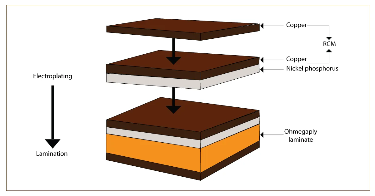
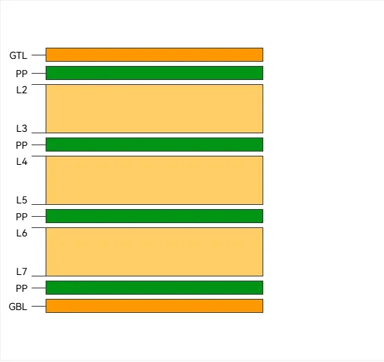
Embedding passives begins with material selection and layer-specific processes tailored to 8-layer stackups. Thin-film resistors form through sputtering or electroless plating of resistive foils onto core layers, followed by photolithography and etching to define values. These 8-layer PCB thin-film resistors offer precise tolerances and stability due to their uniform thickness, typically integrated between signal and plane layers. Capacitors embed via ceramic-filled polymers or thin dielectrics pressed between copper foils, creating distributed capacitance right at the power planes. In an 8-layer board, layers 3-6 often host these elements, with outer layers dedicated to signals and protection. The sequential build-up process—lamination, via formation, and trimming—ensures alignment and electrical connectivity.
Laser trimming adjusts resistor values post-fabrication, compensating for process variations while maintaining layer integrity. This method suits 8-layer PCB embedded resistors because inner layers shield the trim sites from mechanical stress. Electrical performance stems from reduced inductance; passives positioned microns from active circuits cut loop areas that cause EMI. Capacitive embedding lowers equivalent series inductance (ESL), vital for decoupling in high-frequency domains. Engineers must model these effects during design, accounting for dielectric constants and foil thicknesses. The result is a cohesive structure where passives contribute to the board's overall impedance profile.
Performance Benefits of 8-Layer PCB Integrated Passives
8-layer PCB performance improvement arises primarily from minimized parasitics and enhanced signal paths. Discrete passives add via stubs, solder fillet inductance, and pad capacitance that degrade high-speed signals; embedded versions eliminate these by direct layer integration. For instance, 8-layer PCB embedded capacitors provide low-inductance decoupling, stabilizing voltage rails across power planes. Resistors integrated near terminations reduce reflections in controlled-impedance lines. This leads to cleaner eye diagrams and lower bit error rates in data transmission.
Thermal advantages emerge as embedded passives distribute heat evenly through the stackup, leveraging inner planes as heat sinks. Without surface protrusions, airflow improves over the board, aiding convection cooling. Reliability boosts from fewer joints; no reflow soldering means resistance to thermal cycling per IPC-6017 guidelines for embedded circuitry. In vibration-prone environments, the monolithic structure outperforms discrete arrays. Electric engineers observe these gains in simulations, where embedded designs show 20-50% reductions in crosstalk, though exact figures depend on stackup specifics. Overall, 8-layer PCB integrated passives elevate system margins for RF and digital applications.
Another key benefit is size efficiency; an 8-layer board with passives embedded reclaims up to 30% of surface area for logic or memory. This enables slimmer enclosures without performance trade-offs. Power delivery networks benefit from plane-proximate capacitors, slashing voltage droop during transients. These factors compound in multilayer boards, where layer pairing optimizes return paths.
Best Practices for Design and Manufacturing
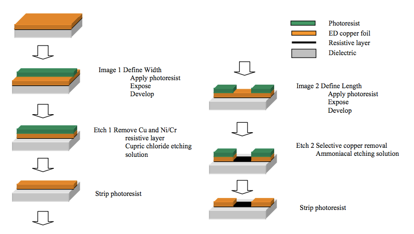
Designers start with stackup planning, assigning inner cores for passives while reserving outer layers for high-speed traces. Symmetrical builds prevent warpage, with core thicknesses matched around the neutral axis. For 8-layer PCB embedded resistors, specify sheet resistivity and geometry in layout files, targeting values via length-to-width ratios. Simulate thermal expansion mismatches between resistive films and dielectrics to avoid delamination. Material datasheets dictate compatibility, favoring low-CTE resins for stability.
Manufacturing follows sequential lamination: photoimage resistive foils, etch, then align with prepregs. Post-laminate trimming uses laser pulses controlled by in-situ resistance monitoring. Vias connect passives to nets without stubs, using blind or buried types common in 8-layer boards. Qualification per J-STD-001 verifies solderless joints and environmental endurance. Engineers iterate prototypes with test coupons for tolerance verification. Documentation includes fab drawings highlighting passive layers for precise processing.
Yield optimization involves process windows: control plating uniformity for thin-film consistency and dielectric thickness for capacitance. Final electrical testing confirms values across temperature ranges. These practices ensure 8-layer PCB performance improvement translates to production reliability.
Challenges and Mitigation Strategies
One challenge is tolerance control; embedded passives demand precise processes to hit 5-10% specs without excessive trimming. Solution: select materials per IPC-4811 and incorporate test structures. Drift under humidity affects polymer types, mitigated by thin-film alternatives with better stability. Integration in 8-layer stackups risks via encroachment; designers route around passive areas with keep-out zones. Cost rises initially for tooling, but volumes amortize savings from fewer placements.
Reliability testing simulates life cycles: thermal shock, bias humidity, and high-temperature storage reveal weaknesses. Embedded capacitors may exhibit micro-cracking if CTE mismatched; balanced stackups resolve this. Engineers address these logically through FEA modeling and coupon data.
Conclusion
Embedded passives transform 8-layer PCBs into efficient platforms for demanding electronics. 8-layer PCB embedded resistors, capacitors, and thin-film variants deliver integration density and performance gains unmatched by discretes. Electric engineers gain tools for superior signal integrity, reliability, and miniaturization. Adhering to standards like IPC-6017 ensures manufacturability. As designs evolve, these technologies will anchor next-generation systems.
FAQs
Q1: What are 8-layer PCB embedded resistors and how are they integrated?
A1: 8-layer PCB embedded resistors integrate thin-film materials like nickel-phosphorus directly into inner layers during fabrication. Processes include deposition, patterning, and laser trimming for precise values. This eliminates discrete parts, reducing parasitics and board size. Engineers specify geometries for desired resistance, ensuring compatibility with stackup materials. Benefits include stable performance in high-density designs.
Q2: How do 8-layer PCB embedded capacitors improve performance?
A2: 8-layer PCB embedded capacitors form between conductive planes using high-K dielectrics, providing low-ESL decoupling. Placed near power rails, they minimize voltage ripple in transients. Integration shortens current loops, enhancing signal integrity over discrete alternatives. In 8-layer boards, they leverage plane pairs for uniform fields. This supports high-speed operation with less EMI.
Q3: What performance improvements come from 8-layer PCB integrated passives?
A3: 8-layer PCB performance improvement from integrated passives includes reduced parasitics, better thermal distribution, and higher reliability without solder joints. Shorter paths lower inductance, aiding RF and digital signals. Space savings allow denser routing. Standards guide qualification for consistent results. Engineers see cleaner waveforms and extended margins.
Q4: Are there best practices for 8-layer PCB thin-film resistors?
A4: For 8-layer PCB thin-film resistors, plan stackups with dedicated cores and symmetrical builds to avoid warpage. Use simulation for thermal matches and tolerances. Manufacturing involves sequential etching and trimming with test coupons. Per industry guidelines, verify stability across conditions. This ensures reliable integration in complex boards.
References
IPC-4811 — Specification for Embedded Passive Device Resistor Materials for Rigid and Multilayer Printed Boards. IPC, 2008
IPC-6017A — Qualification and Performance Specification for Embedded Passive and Active Circuitry. IPC, 2010
IPC-6012E — Qualification and Performance Specification for Rigid Printed Boards. IPC, 2017


