Introduction
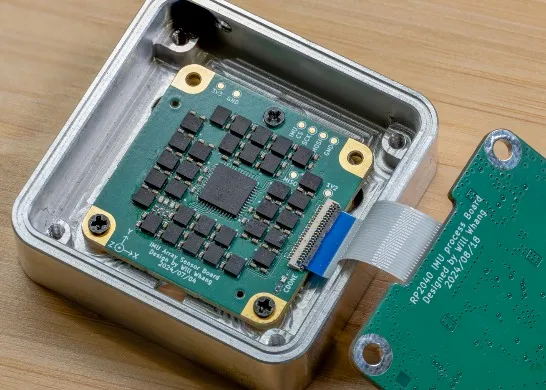
Navigation systems in applications like autonomous vehicles, drones, and robotics rely heavily on inertial measurement units (IMUs) integrated directly onto printed circuit boards (PCBs). These systems demand precise navigation PCB sensor integration to ensure accurate positioning, orientation, and motion tracking under dynamic conditions. Key sensors such as accelerometers, gyroscopes, and magnetometers form the core of these IMUs, providing data on linear acceleration, angular velocity, and magnetic fields respectively. Proper PCB design minimizes noise, mechanical stress, and power issues that can degrade sensor performance. This guide outlines engineering principles and best practices for electric engineers designing high-reliability navigation PCBs. By following structured approaches, designers can achieve robust sensor fusion for real-time navigation.
Key Sensors in Navigation System PCBs
Accelerometers detect linear motion and tilt by measuring specific force, including gravity, making them essential for dead reckoning in GPS-denied environments. Gyroscopes capture angular rates around multiple axes, enabling precise orientation tracking despite vibrations. Magnetometers sense Earth's magnetic field for heading information, compensating for yaw drift in IMUs. In navigation PCB accelerometer, gyroscope, and magnetometer integration, these sensors must operate synergistically through sensor fusion algorithms. Fusion techniques combine raw data to estimate position and attitude, reducing individual sensor errors like accelerometer bias or gyroscope drift. Engineers must consider sensor specifications such as bandwidth, noise density, and full-scale range during selection to match application demands.
Technical Principles of Navigation PCB Sensor Integration
Effective navigation PCB sensor integration begins with PCB layout that isolates sensors from noise sources. Place sensors centrally on the board, away from edges and mounting holes, to reduce mechanical stress from flexing or thermal expansion. Ground planes beneath sensors provide shielding against electromagnetic interference (EMI), while dedicated power planes ensure stable supply voltages. Decoupling capacitors positioned within millimeters of sensor power pins filter high-frequency noise, critical for low-signal outputs from MEMS devices. Signal traces should use differential routing for analog outputs to maintain integrity over distance. Adhering to IPC-2221 guidelines for trace spacing and via placement prevents crosstalk in high-density layouts.
Thermal management plays a pivotal role, as temperature variations affect sensor zero-point stability. Select PCB materials with low coefficients of thermal expansion (CTE) to match sensor packages, minimizing solder joint stress during operation. Vibration isolation through compliant mounting or damping materials preserves accelerometer and gyroscope accuracy in navigation environments. For magnetometers, maintain clearance from ferromagnetic materials and current-carrying traces to avoid hard and soft iron distortions. Power distribution networks must deliver clean, low-noise supplies, often requiring linear regulators post-switching converters. These principles ensure sensors deliver data suitable for fusion algorithms like complementary or Kalman filters.
Best Practices for Navigation PCB Accelerometer Integration
Position accelerometers symmetrically between board fasteners to distribute mounting stresses evenly across the die. Use short, wide traces for power and ground to lower impedance, paired with 0.1 μF and 10 μF ceramic capacitors for broadband decoupling. Avoid placing vias or high-current paths under the sensor footprint, as they induce localized heating and stress. In multilayer boards, dedicate inner layers for ground return paths directly beneath the accelerometer. Implement guard rings around analog outputs to shield from digital noise. These steps enhance signal-to-noise ratio, vital for detecting subtle motions in navigation systems.
Optimizing Gyroscope Placement and Routing on Navigation PCBs
Gyroscopes demand rigid mounting to prevent microphonic effects from board flexure, which mimic rotational rates. Orient the package so sensitive axes align with expected vibration profiles, and reinforce the local area with stitching vias to the ground plane. Route gyroscope outputs as matched-length differential pairs, terminated with resistors matching the sensor's output impedance. Separate digital interfaces like SPI or I2C from analog lines using ground fences to block crosstalk. Thermal vias under the package dissipate heat from internal heaters, maintaining bias stability. Following these practices supports long-term drift compensation in navigation PCB gyroscope designs.
Magnetometer Integration Considerations for Navigation PCBs
Magnetometers require a distortion-free magnetic environment, so position them away from inductors, transformers, and battery cells by at least 10 times the component's largest dimension. Implement calibration routines in firmware to correct for fixed offsets post-assembly. Use shielded enclosures or mu-metal if external fields are unavoidable, while ensuring PCB ground planes do not create eddy current loops. Analog outputs benefit from low-pass filtering directly at the pin to reject high-frequency noise. During layout, simulate magnetic fields from traces using tools compliant with design standards. This integration preserves heading accuracy essential for navigation PCB magnetometer performance.
Implementing Sensor Fusion on Navigation PCBs
Sensor fusion on navigation PCBs processes accelerometer, gyroscope, and magnetometer data to produce attitude and position estimates. Complementary filters blend high-frequency gyroscope data with low-frequency accelerometer and magnetometer inputs for responsive yet stable outputs. Extended Kalman filters model system dynamics, predicting states and correcting with measurements, demanding low-latency processor integration nearby. PCB design supports this by minimizing inter-sensor trace lengths for synchronized sampling and providing ample decoupling for the fusion microcontroller. Partition the board into analog sensor zones and digital processing zones to prevent mutual interference. Robust fusion reduces navigation errors, enabling applications from UAVs to wearable trackers.
Fabrication and Assembly for Reliable Sensor Integration
During fabrication, ensure PCB surfaces meet IPC-6012 qualification for rigid boards, focusing on coplanarity for fine-pitch sensor packages. Assembly follows reflow profiles defined in IPC/JEDEC J-STD-020E to classify and handle moisture-sensitive sensors, preventing popcorning. Bake components prior to reflow if exceeding floor life, and profile ovens for peak temperatures matching sensor ratings. Post-reflow inspection verifies solder joint fillet formation without voids. Selective soldering suits through-hole hybrids, while avoiding excessive flux residues that attract contaminants. These processes yield navigation PCBs resilient to environmental stresses.
Testing and Troubleshooting Navigation PCB Sensors
Validate integration through static and dynamic tests, including bias stability over temperature ramps and Allan variance analysis for noise characterization. Vibration tables simulate operational profiles, quantifying cross-axis sensitivities. Magnetometer calibration involves rotating the assembly in a field-free sphere to map distortions. Common issues like accelerometer offset arise from uneven solder volume; remedy with reflow rework and retest. Gyroscope drift from thermal gradients requires active compensation via onboard heaters. Systematic debugging with oscilloscopes on power rails identifies noise coupling early.
Conclusion
Integrating sensors on navigation system PCBs demands meticulous attention to layout, noise mitigation, and assembly processes for optimal performance. Electric engineers benefit from principles like central placement, shielding, and standard-compliant fabrication to realize accurate IMUs. Navigation PCB sensor fusion elevates raw data into reliable navigation solutions, balancing size, power, and precision. By addressing mechanical, electrical, and thermal challenges, designs withstand real-world demands. This guide equips teams to produce high-fidelity boards for advanced applications.
FAQs
Q1: What are the main challenges in navigation PCB sensor integration?
A1: Navigation PCB sensor integration faces issues like mechanical stress causing zero shifts, EMI corrupting signals, and thermal drift affecting bias. Accelerometers suffer from board flexure, gyroscopes from vibrations, and magnetometers from magnetic distortions. Mitigate with rigid mounting, ground planes, and calibration routines. Adhering to IPC-2221 for layout ensures reliability. Proper decoupling and zoning separate analog and digital sections effectively.
Q2: How does sensor fusion improve navigation PCB performance?
A2: Sensor fusion in navigation PCBs combines accelerometer gravity vectors, gyroscope rates, and magnetometer headings to correct individual errors like drift and noise. Algorithms such as Kalman filters provide robust state estimates for position and orientation. PCB design supports this with low-noise power and short traces for synchronization. This enhances accuracy in dynamic environments like drones. Navigation PCB sensor fusion reduces cumulative errors over time significantly.
Q3: What PCB layout tips optimize navigation PCB accelerometer accuracy?
A3: For navigation PCB accelerometer integration, place the sensor centrally between fasteners to minimize stress. Add decoupling capacitors close to pins and a solid ground plane underneath. Avoid vias and heat sources nearby to prevent thermal gradients. Use low-CTE materials matching the package. Route signals differentially for integrity. These practices lower noise and maintain sensitivity.
Q4: Why follow standards like J-STD-020E for navigation PCB assembly?
A4: IPC/JEDEC J-STD-020E classifies moisture sensitivity for sensors, guiding reflow profiles to avoid delamination. Navigation PCBs with MEMS devices require baking and controlled peaks to protect packages. This prevents defects like cracks during assembly. Compliance ensures high yields and reliability in humid environments. It standardizes processes across teams.
References
IPC-2221 — Generic Standard on Printed Board Design. IPC
IPC-6012E — Qualification and Performance Specification for Rigid Printed Boards. IPC, 2015
IPC/JEDEC J-STD-020E — Moisture/Reflow Sensitivity Classification for Nonhermetic Surface Mount Devices. IPC/JEDEC, 2014


