Introduction
Smart grids represent a transformative approach to power distribution, enabling efficient energy management through continuous data collection and analysis. Printed circuit boards (PCBs) serve as the backbone for integrating sensors that provide real-time insights into voltage levels, current flows, temperature variations, and fault conditions across the grid. Proper PCB integration of smart grid sensors ensures reliable data acquisition amid high-voltage environments and electromagnetic interference. Engineers must address challenges like signal integrity and thermal management to maintain monitoring accuracy. This article explores PCB layout for sensor accuracy, sensor placement for optimal monitoring, data acquisition PCB design, and signal conditioning for smart grid sensors. By following structured engineering principles, designers can enhance grid stability and performance.
The Critical Role of Sensors in Smart Grid PCBs
Sensors in smart grids detect parameters essential for operational oversight, such as power quality and load balancing. Common types include voltage sensors, current sensors, and environmental monitors, all mounted directly on PCBs for compact integration. These components enable phasor measurement units and protective relays to respond instantaneously to anomalies. Without precise sensor data, grid operators risk outages or inefficiencies. PCB integration of smart grid sensors thus bridges the physical grid with digital analytics. Adhering to standards like IPC-2221 for design guidelines ensures that sensor performance aligns with grid demands.
The relevance extends to renewable energy integration, where fluctuating inputs from solar or wind require vigilant monitoring. Sensors on PCBs facilitate predictive maintenance by tracking degradation over time. This setup supports advanced features like demand response and microgrid autonomy. Engineers benefit from modular PCB designs that scale with grid expansions. Ultimately, robust sensor implementation drives the reliability of modern power systems.
Technical Principles of Sensor Integration
Sensor integration on PCBs begins with understanding analog signal paths from detection to processing. Raw sensor outputs, often in millivolts, demand careful routing to prevent attenuation or distortion. Grounding schemes play a pivotal role, separating analog and digital grounds to minimize loops that induce noise. Power supply decoupling capacitors near sensors stabilize voltage rails against fluctuations common in grid environments. Thermal considerations arise from power dissipation in high-current monitoring circuits. These principles form the foundation for accurate real-time data in smart grids.
Electromagnetic compatibility requires shielding traces and components from external fields generated by nearby conductors. Differential signaling preserves signal integrity over longer distances on the PCB. Calibration factors, influenced by layout parasitics, must be modeled during design. Material selection affects dielectric constants, impacting high-frequency responses in current sensors. Engineers apply these mechanisms to achieve sub-percent accuracy in measurements. Compliance with IPC-6012E specifications verifies that the PCB withstands operational stresses like vibration and humidity.
PCB Layout for Sensor Accuracy
PCB layout for sensor accuracy prioritizes short, wide traces for analog signals to reduce resistance and capacitance. Placing sensors close to conditioning circuits minimizes pickup from crosstalk. A solid ground plane under sensitive areas provides a low-impedance return path. Vias should be stitched densely around sensor islands to enhance shielding. Decoupling networks, including ferrite beads, filter high-frequency noise from power lines. These techniques ensure that sensor outputs reflect true grid conditions without artifacts.
Layer stackup influences performance, with dedicated analog layers isolating signals from digital switching noise. Controlled impedance traces maintain signal fidelity for high-speed data acquisition. Thermal vias under power sensors dissipate heat evenly, preventing drift. Designers iterate layouts using simulation to predict parasitics. Following IPC-2221 recommendations for clearance and creepage distances accommodates high-voltage isolation. This methodical approach yields layouts resilient to grid transients.
Routing hierarchies separate high-current paths from low-level sensor lines, avoiding magnetic coupling. Guard traces around analog signals shunt stray fields to ground. Component orientation aligns with airflow for cooling. Final DRC checks confirm adherence to manufacturing tolerances. Such layouts support precision monitoring essential for grid synchronization.
Sensor Placement for Optimal Monitoring
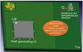
Sensor placement for optimal monitoring involves positioning current sensors near busbars while isolating them from heat sources. Voltage dividers benefit from central locations to average potentials accurately. Temperature sensors require proximity to critical junctions without direct contact that could alter readings. Accessibility for calibration probes influences edge placements. Mechanical stress points, like board flexure areas, demand reinforced mounting. Optimal arrangements balance electrical, thermal, and physical factors for comprehensive coverage.
In multi-sensor arrays, staggering placements avoids mutual interference. Hall-effect sensors for DC currents thrive away from AC fields. Strategic grouping clusters related sensors, shortening interconnects. Simulations predict field distributions to refine positions. Vibration-resistant adhesives secure sensors in dynamic grid nodes. These strategies enhance data granularity for fault localization.
Environmental exposure guides enclosures, with conformal coatings protecting against humidity. Placement near connectors eases field upgrades. Iterative testing validates performance under load. Engineers achieve holistic monitoring through deliberate positioning.
Data Acquisition PCB Design Considerations
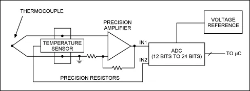
Data acquisition PCB design centers on analog-to-digital converters (ADCs) positioned adjacent to sensors for minimal latency. Multiplexers handle multiple channels efficiently, with anti-aliasing filters per input. Clock distribution uses matched lengths to prevent skew. FIFO buffers manage burst data from transient events. Power domains segregate analog and digital sections with linear regulators. This architecture supports high-sample-rate monitoring in smart grids.
Buffer amplifiers drive ADC inputs without loading sensors. Reference voltage stability relies on low-noise LDOs and bypass capacitors. Oversampling techniques improve resolution amid noise. Layout symmetry in differential pairs boosts common-mode rejection. J-STD-001 guidelines ensure reliable soldering of fine-pitch ADCs. Comprehensive designs capture grid dynamics accurately.
Synchronization across boards uses precision timing crystals. Error-checking checksums validate data streams. Scalable buses like SPI facilitate expansion. Prototyping verifies end-to-end integrity.
Signal Conditioning for Smart Grid Sensors
Signal conditioning for smart grid sensors amplifies weak outputs, filters noise, and linearizes responses. Instrumentation amplifiers provide high gain with low offset for current shunts. Low-pass filters attenuate switching harmonics from inverters. Isolation transformers or optocouplers protect against surges. Chopper stabilization counters drift in precision applications. These circuits precondition signals for robust digitization.
Active rectification handles AC-coupled sensors like Rogowski coils. Offset adjustment accommodates bipolar ranges. Diagnostic loops monitor conditioner health. Component selection favors low-temperature-coefficient parts. PCB traces for conditioned signals employ shielding. Effective conditioning elevates raw data to actionable insights.
Feedback loops enable auto-zeroing. Multi-stage designs cascade filtering for sharp roll-off. Compliance testing confirms bandwidth margins. Integrated solutions streamline board real estate.
Common Challenges and Troubleshooting
Noise injection from ground bounce plagues sensor readings, resolved by single-point grounding schemes. Thermal runaway in power sensors demands enhanced copper pours and vias. Solder joint cracks under vibration require underfill or compliant pads per J-STD-001. EMI susceptibility tests identify weak shielding. Calibration shifts post-assembly signal mechanical stresses. Systematic debugging restores accuracy.
Component mismatch induces offsets, mitigated by matched pairs. Power supply ripple demands pi-filters. Firmware glitches mimic hardware faults, necessitating scope captures. Field returns highlight humidity ingress, prompting better IP ratings. Proactive measures like design reviews prevent recurrence.
Conclusion
Implementing sensors on smart grid PCBs demands meticulous attention to layout, placement, data acquisition, and conditioning for real-time reliability. Key practices like noise isolation, precise routing, and standards compliance yield high-fidelity monitoring. Engineers equipped with these strategies enhance grid resilience against faults and inefficiencies. Future advancements in materials will further refine integrations. Prioritizing PCB design fundamentals ensures scalable, durable solutions.
FAQs
Q1: What factors influence PCB layout for sensor accuracy in smart grids?
A1: PCB layout for sensor accuracy hinges on minimizing trace lengths, implementing ground planes, and separating analog from digital sections. Shielding and decoupling reduce noise interference critical in high-EMI environments. Adhering to IPC-2221 guidelines for spacing prevents crosstalk. Thermal management via pours maintains stability. These elements ensure precise voltage and current readings.
Q2: How does sensor placement for optimal monitoring affect smart grid performance?
A2: Sensor placement for optimal monitoring positions devices to capture representative data while avoiding heat and fields. Close proximity to points of interest shortens paths, enhancing signal integrity. Staggered arrays cover zones comprehensively. Mechanical securing withstands vibrations. Proper placement supports rapid fault detection and load balancing.
Q3: Why is signal conditioning essential in PCB integration of smart grid sensors?
A3: Signal conditioning amplifies, filters, and isolates weak sensor outputs for ADC compatibility. It rejects grid noise and linearizes nonlinear responses. Instrumentation amps provide CMRR for accuracy. Surge protection safeguards circuits. This step is vital for reliable real-time data in dynamic power systems.
Q4: What role does data acquisition PCB design play in smart grid applications?
A4: Data acquisition PCB design integrates ADCs near sensors for low-latency capture. Multiplexing and buffering handle multi-channel inputs efficiently. Stable references and clocks ensure precision. Isolated domains prevent corruption. Optimized designs enable high-resolution monitoring of grid parameters.
References
IPC-2221 — Generic Standard on Printed Board Design. IPC
IPC-6012E — Qualification and Performance Specification for Rigid Printed Boards. IPC, 2015
J-STD-001 — Requirements for Soldered Electrical and Electronic Assemblies. IPC/JEDEC
IEC 61850 — Communication networks and systems for power utility automation. IEC


