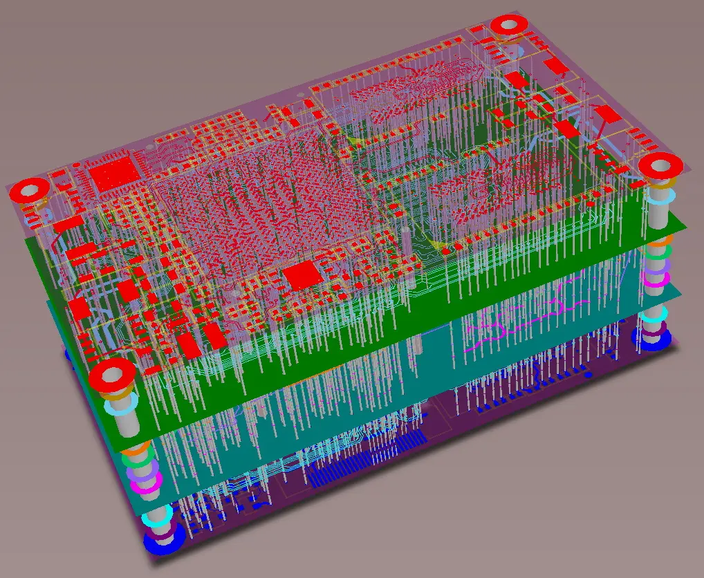
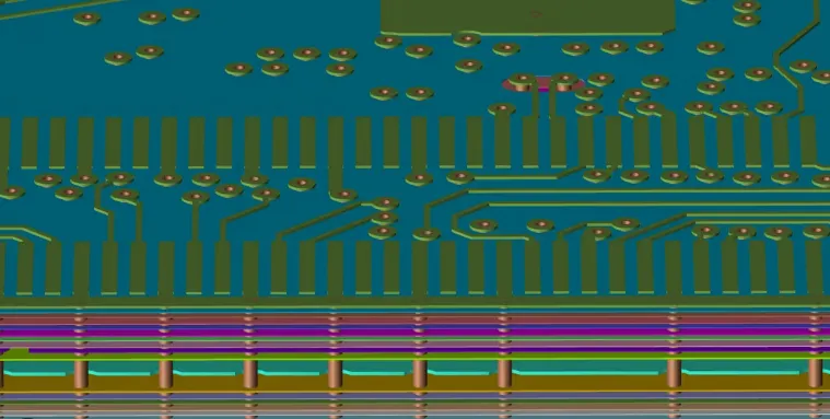
In the rapidly evolving landscape of modern electronics, the demand for smaller, faster, and more powerful devices is relentless. At the heart of this technological revolution lies the printed circuit board (PCB). However, gone are the days when a simple single-sided or double-sided board could handle the complex routing and electrical requirements of advanced circuitry. Today, the foundation of any high-performance electronic device is a meticulously engineered multilayer PCB stackup.
A multilayer stackup is much more than just a physical arrangement of copper and insulating layers. It is a critical component of the circuit design itself. The stackup configuration dictates the board's signal integrity, power distribution efficiency, electromagnetic compatibility (EMC), and thermal performance. A well-designed stackup can prevent a multitude of operational failures, while a poorly planned one will inevitably lead to costly revisions, degraded performance, and failed compliance testing.
This comprehensive pillar page serves as your ultimate guide to mastering multilayer PCB stackup design. We will explore the anatomy of a stackup, the critical elements that influence performance, industry-standard configurations, and the best practices required to navigate complex challenges such as thermal management, high-frequency routing, and comprehensive testing.
1. The Anatomy of a Multilayer PCB Stackup
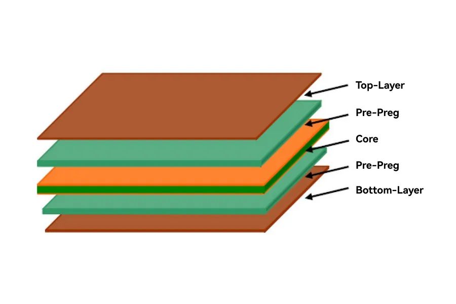
Before diving into advanced design strategies, it is essential to understand the physical building blocks of a multilayer PCB. A stackup is formed by laminating alternating layers of conductive copper and insulating dielectric materials under high temperature and pressure.
The three primary components include:
- Copper Foil: The conductive layers used for routing signals, distributing power, and providing ground references.
- Core: A rigid, fully cured piece of dielectric material (commonly FR-4) with copper foil bonded to either one or both sides. The core forms the sturdy backbone of the internal layers.
- Prepreg: A layer of fiberglass cloth impregnated with uncured resin. During the lamination process, the prepreg melts, flows, and bonds the core layers together, eventually curing into a solid dielectric.
The primary goal of stackup design is to arrange these materials symmetrically to prevent mechanical warping while meeting exact electrical characteristics.
2. Why Stackup Architecture is Critical
The transition from a schematic to a physical board introduces parasitic inductance, capacitance, and resistance. The multilayer stackup is your primary weapon for controlling these parasitics.
A strategic stackup achieves three main objectives:
1. Signal Integrity (SI): By carefully controlling the distance between signal layers and reference planes, you can maintain precise characteristic impedance, preventing signal reflections and degradation.
2. Power Integrity (PI): A good stackup provides a low-impedance power delivery network (PDN), ensuring stable voltage levels across the board even under transient loads.
3. Electromagnetic Compatibility (EMC): By burying high-speed signal layers between continuous ground or power planes, you create a natural Faraday cage that contains internal electromagnetic radiation and shields the board from external interference.
3. Core Elements of Multilayer Stackup Optimization
To truly optimize a multilayer PCB, designers must address several interrelated subsystems within the board. Below are the foundational pillars of stackup design.
The Backbone: Power and Ground Planes
The arrangement of power and ground layers is arguably the most critical decision in stackup design. Continuous reference planes provide a clear, low-impedance return path for signals, which is vital for minimizing electromagnetic interference (EMI) and cross-talk. Furthermore, adjacent power and ground planes create beneficial inter-plane capacitance, acting as a high-frequency decoupling capacitor for the power delivery network. For designers looking to dive deeper into how plane arrangement dictates return paths and board stability, highly recommend understanding power and ground planes in multi-layer PCBs as it forms the bedrock of reliable electrical performance.
Material Selection and Dielectric Properties
The materials you choose for your core and prepreg layers define the electrical environment of your board. Two critical parameters to consider are the Dielectric Constant (Dk) and the Dissipation Factor (Df). Dk affects the speed of signal propagation and impedance calculations, while Df dictates how much signal energy is lost as heat within the dielectric.
Additionally, the physical thickness of these materials heavily influences trace widths required for impedance matching. By optimizing dielectric thickness in multilayer PCBs, engineers can fine-tune impedance profiles, minimize inter-layer cross-talk, and achieve the desired overall board thickness without compromising mechanical stability.
Interconnectivity: Via Design Strategies
As layer counts increase, moving signals vertically between layers becomes a complex challenge. Vias—the plated holes that connect different layers—are essential, but they introduce impedance discontinuities (stubs) that can wreak havoc on high-speed signals.
Designers must choose between standard through-hole vias, blind vias (connecting an outer layer to an inner layer), buried vias (connecting internal layers only), and advanced high-density interconnect (HDI) microvias. Each via type impacts routing density, signal integrity, and manufacturing costs. By mastering via design in multilayer PCBs, you can ensure seamless layer transitions, minimize signal reflections, and maximize the real estate available on your board.
Thermal Management Considerations
Modern electronics pack immense processing power into tiny form factors, resulting in significant heat generation. Multilayer PCBs present a unique thermal challenge because internal layers (especially prepreg/core materials) act as thermal insulators, trapping heat inside the board.
If heat is not efficiently removed, it can lead to material delamination, altered dielectric properties, and catastrophic component failure. Utilizing heavy copper layers, strategic thermal vias, and heat-dissipating core materials are vital strategies for managing heat in high power multilayer PCB designs. A thermal-aware stackup ensures that high-current paths have adequate copper weight and that heat is efficiently funneled away from critical components to outer surface heat sinks.
High-Frequency and RF Implications
When designing for Radio Frequency (RF) and microwave applications, standard stackup rules often fall short. High-frequency signals are incredibly sensitive to minor variations in dielectric thickness, copper surface roughness, and via transitions. The "skin effect" pushes current to the outer edges of the copper traces, increasing resistance and loss.
For these specialized boards, designers must utilize specialized, low-loss laminate materials (such as PTFE/Teflon or Rogers materials) and employ exact microstrip or stripline routing topologies. Implementing a specialized multilayer PCB design for RF applications ensures minimized insertion losses, precise impedance matching, and stringent isolation between noisy digital sections and sensitive analog/RF circuits.
4. Standard Multilayer Stackup Configurations
While custom stackups are common for highly specialized applications, the industry relies on several standard configurations that balance cost, manufacturability, and performance. Here is an overview of how layers are typically assigned in common board types:
The 4-Layer Stackup
The 4-layer board is a massive upgrade over a 2-layer board, primarily because it allows for dedicated power and ground planes. A standard configuration is:
Advantage: The solid ground plane on layer 2 provides a tightly coupled return path for high-speed signals on the top layer, significantly reducing EMI.
The 6-Layer Stackup
When routing density increases, 6 layers become necessary. A 6-layer board provides excellent shielding for sensitive signals. A preferred configuration is:
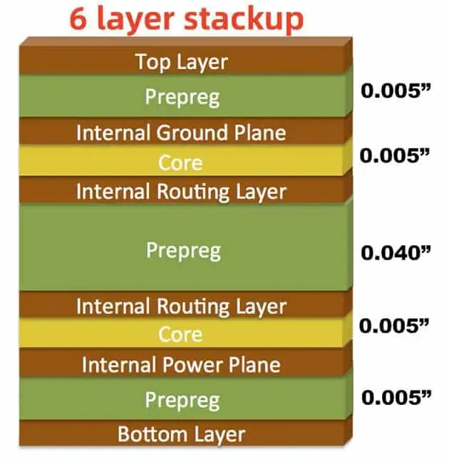
Advantage: Internal signal layers are buried between two solid reference planes, providing maximum shielding against external noise and preventing radiation.
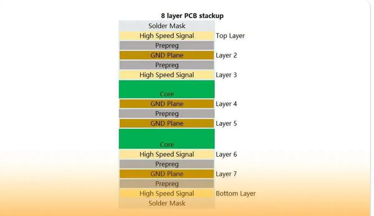
The 8-Layer Stackup (and Beyond)
For complex high-speed digital designs (like servers, advanced IoT gateways, and complex RF equipment), 8 or more layers are required. An 8-layer stackup allows for multiple power domains and superior EMC control.
Advantage: This layout ensures that every single signal layer is adjacent to at least one solid ground plane. Furthermore, having adjacent Power and Ground planes (Layers 4 and 5) maximizes inter-plane capacitance for excellent power integrity.
5. Best Practices for Designing a Winning Stackup
To consolidate your approach to multilayer PCB design, keep these expert rules of thumb in mind:
- Always maintain stackup symmetry: Symmetrical material distribution from the center of the board out prevents bowing and twisting during the high-heat wave soldering or reflow processes.
- Keep signal layers adjacent to reference planes: Never route high-speed signals between two other signal layers (broadside coupling). Always pair a signal layer with a solid ground or power plane to guarantee a tight return path.
- Route orthogonally on adjacent layers: If you must have adjacent signal layers, ensure the traces on one layer run perpendicular (orthogonally) to the traces on the other layer. This minimizes cross-talk.
- Avoid splitting reference planes underneath high-speed traces: Routing a signal over a split plane creates a massive impedance discontinuity and forces the return current to find a longer, noisier path, leading to severe EMI issues.
6. Ensuring Reliability: Validation and Testing
Even the most mathematically perfect stackup design in your CAD tool requires rigorous physical validation. The manufacturing process involves tolerances—dielectrics might be slightly thicker or thinner, and copper etching is never 100% perfect. These microscopic deviations can throw off your impedance calculations or compromise structural integrity.
To ensure your multilayer board functions as intended, physical validation protocols such as Time Domain Reflectometry (TDR) for impedance testing, Vector Network Analyzers (VNA) for RF performance, and Automated Optical Inspection (AOI) must be employed. Recognizing the importance of test and measurement in multilayer PCB development is what separates standard prototypes from production-ready, highly reliable commercial products. Thorough testing validates the mathematical models of your stackup and guarantees long-term reliability in the field.
Conclusion
Mastering the multilayer PCB stackup is a foundational skill for any modern hardware engineer. The stackup is the physical and electrical foundation upon which your entire circuit rests. By carefully orchestrating the arrangement of copper, selecting the right dielectric materials, optimizing via structures, and planning for thermal and high-frequency demands, you transition from simply "connecting the dots" to designing robust, high-performance electronics.
We encourage you to explore the specialized guides linked throughout this pillar page to deepen your expertise in specific areas—from RF design to complex thermal management. A well-planned stackup is your first, best defense against EMI, signal degradation, and power delivery failures. Plan it wisely, test it rigorously, and your designs will perform flawlessly in the real world.


