Introduction
High-speed data transmission in modern printed circuit boards demands precise control over electromagnetic interference to maintain reliable performance. As data rates increase, engineers encounter significant challenges from high-speed data EMI, which can degrade signal integrity and lead to system failures. Electromagnetic interference arises from rapid signal transitions that generate high-frequency emissions, coupling into adjacent traces and causing errors in data transmission. Effective EMI shielding solutions become essential for preserving the quality of differential signaling and minimizing crosstalk between channels. This article explores the principles behind high-frequency EMI in PCBs and provides practical strategies for electric engineers to implement robust shielding techniques. By understanding these mechanisms, designers can optimize PCB layouts for superior signal integrity EMI performance.
Understanding EMI in High-Speed Data Transmission
Electromagnetic interference in high-speed data transmission refers to unwanted noise that disrupts signal waveforms, primarily through crosstalk, radiated emissions, and conducted coupling. Crosstalk occurs when energy from an aggressor trace induces voltage or current in a victim trace, with near-end and far-end effects varying based on trace proximity and length. High-frequency EMI becomes prominent at data rates exceeding gigabits per second, where harmonic frequencies extend into the GHz range, making standard PCB materials and layouts insufficient. Signal integrity EMI compromises eye diagrams, bit error rates, and overall system reliability, particularly in applications like telecommunications and computing. Engineers must prioritize reducing crosstalk early in the design phase to ensure clean data transmission across multiple channels. The relevance of these issues grows with denser interconnects, where minimizing loop areas and maintaining impedance control are foundational.
Key Causes of EMI and Crosstalk in PCBs
High-speed signals propagate as fast-rising edges with significant spectral content at high frequencies, leading to unintended radiation from trace discontinuities like vias and bends. Crosstalk arises mainly from capacitive and inductive coupling between parallel traces, exacerbated by insufficient spacing or lack of reference planes. Differential signaling, while inherently more resilient due to common-mode rejection, still suffers if shielding is inadequate, allowing external noise to convert to differential mode. High-frequency EMI also stems from power distribution networks, where switching currents create return path imbalances and ground bounce. Poor stackup design amplifies these effects, as signal layers distant from ground planes experience higher impedance and radiation. Identifying these causes through simulation and measurement guides effective mitigation strategies.
Technical Principles of EMI Shielding
Shielding works by providing a low-impedance path for currents and blocking electromagnetic fields through conductive barriers. In PCBs, ground planes act as primary shields by returning currents close to signal traces, reducing loop areas and radiated emissions. For differential signaling shielding, paired traces with adjacent ground or power planes confine fields, minimizing coupling to neighboring signals. High-frequency EMI attenuation relies on skin effect, where currents flow on conductor surfaces, making thin shielding layers effective above certain frequencies. Guard traces or stitching vias further enhance isolation by interrupting coupling paths and providing Faraday cage-like enclosures at the board level. These principles align with design guidelines in IPC-2221B, emphasizing controlled environments for high-speed traces.
PCB Stackup Strategies for EMI Reduction
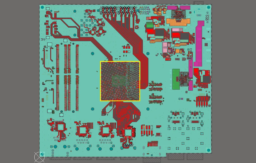
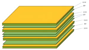
Optimal stackup design places high-speed signal layers adjacent to continuous ground planes, ensuring broadside coupling that suppresses common-mode radiation. Symmetric structures, such as signal-ground-signal-ground, balance impedance and minimize crosstalk between layers. For multilayer boards, core dielectrics with low loss tangents reduce high-frequency EMI propagation losses. Engineers should allocate dedicated planes for power and ground, segmented to avoid slots that act as antennas. Vias fenced along edges connect planes, forming shielded compartments for sensitive data transmission. This approach significantly improves signal integrity EMI by confining fields within the board.
Routing Techniques to Minimize Crosstalk
Proper trace routing keeps high-speed pairs tightly coupled with minimal length mismatch, while maintaining separation from adjacent aggressors. Differential pairs benefit from shielding with grounded traces on both sides or embedded within ground plane cutouts. Reducing crosstalk involves orthogonal routing on adjacent layers to minimize parallel runs and capacitive coupling. Bend radii should exceed three times trace width to avoid impedance discontinuities that radiate EMI. Length-matched meanders for skew control must incorporate shielding to prevent intra-pair imbalance. These techniques ensure robust data transmission under high-speed conditions.
Advanced Shielding Methods for High-Frequency Applications
Embedded shielding layers, such as metal pours or selective plating, create barriers within the PCB for isolating critical channels. For extreme high-frequency EMI, via fences around sensitive areas form effective cages, with spacing less than one-tenth the wavelength of concern. Ferrite beads and capacitors on power lines filter conducted noise before it couples to signals. Differential signaling shielding extends to connectors with twisted pairs transitioning smoothly to PCB launches. Compliance with IPC-2141A aids in calculating impedances that support these shielding configurations. Combining these methods yields comprehensive protection for data transmission integrity.
Best Practices for Implementation
Begin with full-wave simulations to predict EMI hotspots before layout finalization. Maintain trace widths and spacings consistent with target impedances, using field solvers for verification. Place decoupling capacitors near IC pins to shunt high-frequency currents locally. Segregate analog and digital sections with moats or ground splits to prevent noise migration. Post-layout reviews should check return path continuity and loop minimization. Fabricators appreciate designs adhering to IPC-2251 guidelines for high-speed packaging, ensuring manufacturability alongside EMI performance.
Troubleshooting Common EMI Issues
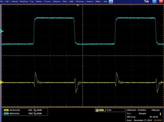
When high-speed data EMI manifests as intermittent errors, inspect eye patterns for closure due to jitter or attenuation. Excessive crosstalk often traces to unshielded parallel runs; remedy with rerouting or added ground fills. Signal integrity EMI from ground bounce requires enhanced decoupling and plane stitching. High-frequency EMI radiation points to slot antennas in planes; fill gaps with pours or jumps. Differential signaling shielding failures stem from asymmetric routing; realign pairs meticulously. Systematic measurements with near-field probes pinpoint sources for targeted fixes.
Conclusion
Effective EMI shielding solutions are critical for high-speed data transmission, directly impacting signal integrity and system reliability. By leveraging ground planes, optimized stackups, and precise routing, engineers can substantially reduce crosstalk and high-frequency EMI. Differential signaling shielding enhances resilience, while adherence to proven principles ensures scalable designs. Implementing these strategies minimizes risks in dense, high-performance PCBs. Electric engineers equipped with these insights can deliver boards that excel in demanding environments. Prioritizing EMI from the outset yields robust data transmission outcomes.
FAQs
Q1: What causes high-speed data EMI in PCB designs?
A1: High-speed data EMI primarily results from fast edge rates generating high-frequency harmonics that radiate or couple to nearby traces. Crosstalk amplifies this through capacitive and inductive mechanisms between parallel conductors. Inadequate reference planes allow loop currents to emit noise, degrading signal integrity EMI. Proper stackup and shielding mitigate these effects effectively.
Q2: How does differential signaling shielding improve data transmission?
A2: Differential signaling shielding confines magnetic and electric fields between pair traces and adjacent ground planes, rejecting common-mode noise. This reduces susceptibility to external high-frequency EMI and minimizes intra-pair imbalance. Guard traces or via fences further isolate pairs, lowering crosstalk. Engineers achieve cleaner eye openings and lower bit error rates in high-speed applications.
Q3: What are key methods for reducing crosstalk in high-speed PCBs?
A3: Reducing crosstalk involves increasing trace spacing, using orthogonal routing on layers, and placing ground planes adjacent to signals. Shielding with grounded traces between aggressors interrupts coupling paths. Length matching and controlled impedance prevent reflections that exacerbate noise. These practices preserve signal integrity EMI during data transmission.
Q4: Why is stackup design crucial for high-frequency EMI control?
A4: Stackup design positions signal layers near continuous ground planes to minimize return path inductance and radiation. Symmetric arrangements balance fields, curbing high-frequency EMI emissions. Low-loss dielectrics attenuate propagation losses. This foundation supports reliable data transmission and differential signaling shielding.
References
IPC-2221B — Generic Standard on Printed Board Design. IPC, 2012
IPC-2141A — Design Guide for High-Speed Controlled Impedance. IPC, 1996
IPC-2251 — Design Guide for the Packaging of High Speed Electronic Circuits. IPC, 2003


