Introduction
In modern high-speed PCB designs, PCB crosstalk emerges as a critical challenge that can compromise signal integrity and overall system performance. As operating frequencies increase and trace densities rise, unwanted signal coupling between adjacent traces becomes more pronounced, leading to noise, timing errors, and potential bit flips. Engineers must grasp the fundamentals of this phenomenon to implement effective mitigation strategies during the routing phase. This article delves into the principles of PCB crosstalk, its causes, and proven techniques for reduction, including trace spacing for crosstalk, guard traces, differential signaling, and methods for reducing near-end crosstalk. By applying these structured approaches, designers can achieve reliable operation in demanding applications such as telecommunications, computing, and automotive electronics. Understanding these elements ensures compliance with performance expectations and minimizes costly redesigns.
What Is PCB Crosstalk and Why It Matters
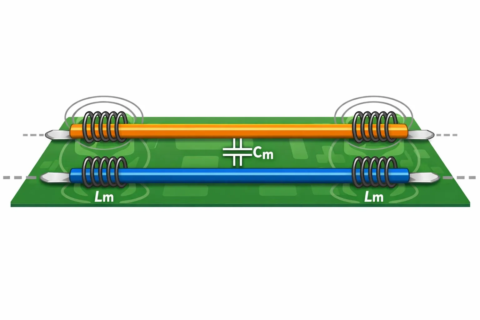
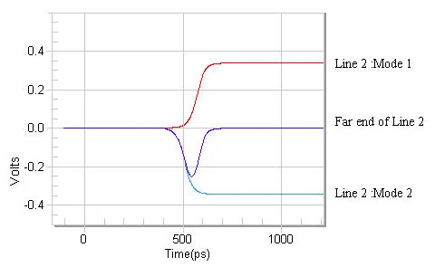
PCB crosstalk refers to the unintentional transfer of electromagnetic energy between adjacent traces on a printed circuit board, manifesting as noise on a victim trace due to activity on an aggressor trace. This coupling occurs primarily through capacitive, inductive, or electromagnetic mechanisms, where electric fields or magnetic fields link the traces. Near-end crosstalk, or NEXT, appears at the same end of the traces as the aggressor signal source, while far-end crosstalk, or FEXT, occurs at the opposite end. In high-speed designs, even short parallel runs can induce significant interference, degrading eye diagrams and increasing bit error rates. The relevance intensifies with rising data rates beyond gigabits per second, where signal rise times approach nanoseconds, amplifying coupling effects.
The implications extend beyond mere noise addition. Excessive PCB crosstalk can lead to electromagnetic interference emissions that violate regulatory limits, trigger false triggering in logic circuits, and cause timing skew in synchronized systems. For electric engineers, neglecting crosstalk risks field failures, extended debug cycles, and non-compliance with performance specifications. In multilayer boards, interactions across layers compound the issue, demanding proactive design considerations from the outset. Prioritizing crosstalk mitigation preserves signal fidelity, enhances power efficiency, and supports scalable architectures in evolving technologies.
Mechanisms of Crosstalk in PCB Trace Routing
Crosstalk arises from electromagnetic coupling between traces, with capacitive coupling dominating when traces run parallel over extended lengths. In this scenario, the changing voltage on the aggressor trace induces a displacement current on the victim trace through overlapping electric fields, proportional to the mutual capacitance and the aggressor's dv/dt. Inductive coupling complements this by linking magnetic fields from the aggressor's current changes, inducing voltage via mutual inductance, especially in unbalanced impedance environments. The coupling strength depends on factors such as trace separation, length of interaction, height above reference planes, and dielectric properties of the substrate. Engineers observe that closer spacing and longer parallel sections exponentially increase crosstalk amplitude.
Near-end crosstalk typically exhibits forward coupling with minimal attenuation, while far-end crosstalk involves both forward and backward waves that partially cancel in balanced systems. Transmission line theory models these effects using coupled microstrip or stripline equations, where characteristic impedance mismatches exacerbate reflections and noise. Substrate materials with lower dielectric constants reduce fringing fields, offering partial mitigation, but routing geometry remains paramount. In dense layouts, via transitions and bends introduce additional discontinuities that couple energy unpredictably. Recognizing these mechanisms guides simulation-driven verification before fabrication.
Factors Influencing Crosstalk Severity
Trace geometry plays a pivotal role, as narrower traces with finer spacing heighten field overlap despite reduced individual capacitance. Parallel run lengths beyond a few millimeters become critical thresholds, where coupling transitions from negligible to dominant. Impedance control interacts here, as mismatched lines reflect energy, reinforcing crosstalk peaks. Layer stackup influences vertical coupling, with microstrip traces more susceptible than embedded striplines due to greater field exposure. Environmental factors like temperature variations alter dielectric constants, subtly shifting coupling levels over time.
Return path proximity modulates inductive effects, as nearby ground planes confine magnetic fields effectively. Signal characteristics, including edge rates and duty cycles, determine excitation strength, with faster transitions yielding higher noise voltages. Multi-aggressor scenarios compound interference, creating complex noise spectra that simulations must capture accurately. Engineers quantify these via time-domain reflectometry or vector network analysis post-layout.
Practical Solutions for Mitigating Crosstalk
Effective crosstalk reduction begins with optimizing trace spacing for crosstalk, adhering to guidelines that scale separation with trace width and speed requirements. A common heuristic positions adjacent signal traces at least three times the trace width apart to attenuate coupling below acceptable thresholds, balancing density with integrity. Increasing spacing reduces mutual capacitance and inductance linearly at first, then more effectively beyond critical distances. IPC-2221 provides foundational spacing rules adaptable for signal integrity, emphasizing minimum clearances based on voltage and environmental factors.
Guard traces offer a targeted shield, inserted between sensitive pairs and connected to ground via dense stitching. These grounded conductors absorb induced currents, shunting noise before it reaches victims, particularly effective against inductive coupling. Stitching vias every few millimeters ensure low-impedance paths, preventing resonance. In constrained areas, partial guard traces still yield benefits over unshielded runs.
Differential signaling stands out for its inherent rejection of common-mode noise, converting crosstalk into balanced differential errors that receivers cancel. Paired traces carry complementary signals, with controlled intra-pair spacing and length matching to maintain impedance symmetry. This approach excels in high-speed serial links, where single-ended alternatives falter. Optimal edge coupling within pairs minimizes external susceptibility while maximizing internal balance.
Advanced Routing Best Practices
Route aggressor and victim traces orthogonally where possible to minimize parallel overlap, limiting interaction lengths under signal rise times. Segregate high-speed signals onto dedicated layers with adjacent ground planes, confining fields and reducing broadside coupling. Symmetry in routing preserves differential integrity, avoiding bends that skew pair lengths. Pre-layout planning allocates routing channels with spacing buffers, verified through field solver tools.
Length detuning intentionally mismatches parallel aggressor-victim runs to decorrelate noise peaks temporally. Solid reference planes beneath traces provide return paths, diminishing loop areas and inductive coupling. For multilayer boards, symmetric stackups with plane pairs enhance isolation.
Troubleshooting Crosstalk in Designs
Suspect PCB crosstalk when eye openings narrow, jitter increases, or unexpected spurs appear in spectra. Time-domain simulations reveal coupling peaks, correlated with layout geometries. Measurements using TDR or VNA confirm NEXT/FEXT levels against budgets. Iterative fixes prioritize spacing adjustments before guard additions.
Common pitfalls include overlooked via coupling or plane splits disrupting returns. Post-fabrication, probing with active loads quantifies noise susceptibility.
Conclusion
Mastering PCB crosstalk requires a systematic grasp of coupling physics and layered mitigation tactics. From trace spacing for crosstalk and guard traces to differential signaling and reducing near-end crosstalk, these strategies form a robust toolkit for electric engineers. Integrating them early in design workflows, informed by standards like IPC-2221, yields high-yield, performant boards. Consistent application across projects minimizes risks, accelerates time-to-market, and upholds signal integrity in high-speed realms.
FAQs
Q1: What is the role of trace spacing for crosstalk in PCB design?
A1: Trace spacing for crosstalk directly controls capacitive and inductive coupling by reducing field overlap between adjacent conductors. Wider separations attenuate noise voltage proportionally, with guidelines suggesting multiples of trace width for high-speed signals. Engineers balance this against density constraints, simulating impacts to meet integrity budgets. Proper spacing prevents bit errors and EMI in dense layouts.
Q2: How do guard traces help in reducing near-end crosstalk?
A2: Guard traces, grounded between signal pairs, intercept induced fields, converting crosstalk energy to harmless ground currents. Via stitching ensures effective shunting, particularly for NEXT where noise peaks locally. This passive shielding adds minimal area overhead while boosting isolation by 10-20 dB in simulations. Implementation suits critical nets in multilayer boards.
Q3: Why is differential signaling effective against PCB crosstalk?
A3: Differential signaling transmits complementary signals on paired traces, rejecting common-mode crosstalk at the receiver through subtraction. Tight intra-pair coupling enhances this immunity, while external spacing protects against imbalance. It thrives in serial protocols, simplifying equalization needs. Layout precision in length and impedance matching is essential for peak performance.
Q4: What are key steps for reducing near-end crosstalk in routing?
A4: Prioritize orthogonal routing to shorten parallels, enforce spacing rules, and deploy ground planes. Guard traces and differential pairs target persistent issues. Verify via pre- and post-layout simulations correlating to measurements. Standards like IPC-2221 guide baseline clearances, ensuring scalable mitigation.
References
IPC-2221B — Generic Standard on Printed Board Design. IPC, 2003
IPC-6012E — Qualification and Performance Specification for Rigid Printed Boards. IPC, 2017
J-STD-001H — Requirements for Soldered Electrical and Electronic Assemblies. IPC, 2018


