Introduction
Electromagnetic interference poses a significant challenge in the design of consumer electronics, where compact layouts and high-speed signals amplify the risk of emissions and susceptibility. Optimizing EMI shielding ensures devices operate reliably while meeting stringent regulatory requirements like FCC compliance EMI and CE marking EMI. Engineers must integrate shielding strategies early in the PCB design process to contain radiated and conducted noise effectively. This approach not only reduces EMI in devices but also streamlines compliance testing, avoiding costly redesigns. As consumer products such as smartphones, wearables, and smart home gadgets proliferate, mastering consumer product shielding becomes essential for market entry. The following sections explore the principles, practices, and regulatory context to guide electric engineers in achieving robust EMI performance.
Understanding EMI in Consumer Electronics and Its Impact
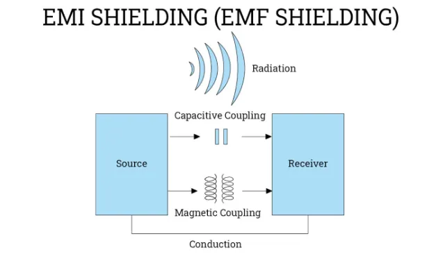
Electromagnetic interference refers to unwanted electromagnetic energy that disrupts electronic circuits, manifesting as conducted noise through power lines or radiated emissions through the air. In consumer electronics, sources like switching regulators, clock oscillators, and high-speed data interfaces generate broadband noise that can exceed limits during compliance testing. Without proper mitigation, this EMI leads to signal integrity issues, such as crosstalk between traces or false triggering in digital logic. Regulatory bodies enforce limits to prevent interference with broadcast services and other devices, making consumer electronics EMI a critical design constraint. Effective shielding maintains device functionality in dense environments, like homes filled with multiple wireless gadgets. Engineers prioritize EMI control to balance performance, size, and cost in these applications.
Key Mechanisms of EMI Generation and Propagation in PCBs
EMI arises primarily from rapid voltage or current changes creating electric and magnetic fields that couple to nearby conductors. On PCBs, large current loops formed by poor routing act as antennas, radiating energy proportional to the loop area and frequency. High-edge-rate signals from processors exacerbate this, with harmonics extending into GHz ranges relevant to FCC and CE tests. Ground bounce and return path discontinuities further amplify emissions by forcing currents to spread across layers. Shielding works by reflecting or absorbing these fields, with effectiveness depending on material conductivity, thickness, and enclosure continuity. Understanding these mechanisms allows engineers to target interventions precisely, such as minimizing loop areas through symmetric routing.
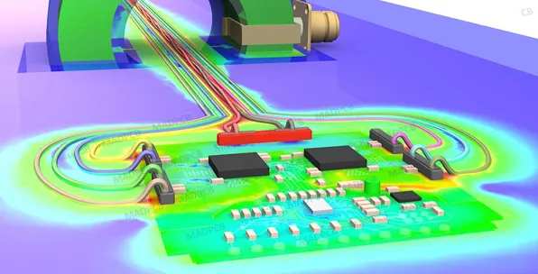
Skin effect confines currents to conductor surfaces at high frequencies, influencing shield design where thickness must exceed skin depth for optimal attenuation. Cavity resonances occur when shield dimensions match wavelengths, potentially worsening emissions unless damped with lossy materials or internal partitions. Coupling modes include near-field magnetic induction between inductors and far-field radiation from traces, each requiring tailored countermeasures. Compliance with standards like IEC 61000-4-3 for radiated immunity highlights the need to model these interactions during design. By simulating field propagation, engineers predict and mitigate hotspots before prototyping.
Regulatory Requirements for FCC Compliance EMI and CE Marking EMI
FCC Part 15 Class B limits govern unintentional radiators in the US, specifying peak and average emissions from 30 MHz to 1 GHz for consumer products. Devices must demonstrate compliance through accredited testing, with shielding critical to suppress radiated emissions from enclosures and cables. In Europe, the EMC Directive under CE marking EMI references harmonized standards like EN 55032 for multimedia emissions, demanding both emissions and immunity verification. Battery-powered consumer electronics face relaxed conducted limits but stringent radiated ones due to portable nature. Reducing EMI in devices ensures pass rates, as failures often trace to enclosure apertures or poor grounding. Engineers align designs iteratively with these thresholds, incorporating margin for production variations.
Compliance testing involves open-area sites or semi-anechoic chambers, measuring maximum emissions under worst-case configurations like maximum load. Pre-compliance scans using spectrum analyzers guide shielding refinements, focusing on peaks from clocks or power supplies. CE marking EMI extends to immunity against ESD, surges, and RF fields per IEC 61000-4 series, where shielding prevents upsets in sensitive analog sections. Documentation of design mitigations supports declarations of conformity. Global harmonization eases multi-market entry, but region-specific tweaks remain necessary.
Best Practices for Consumer Product Shielding and Reducing EMI in Devices
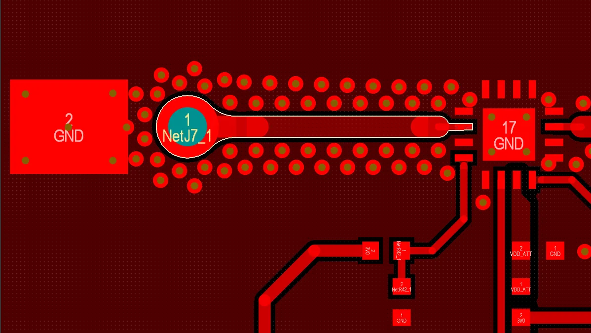
Implement solid ground planes on inner layers adjacent to signal planes to provide low-impedance return paths and image plane shielding. Stitch vias around sensitive areas form via fences, creating virtual walls that block slotline radiation. Route high-speed signals between ground planes with controlled impedance, minimizing discontinuities at vias and bends. Separate analog and digital sections with guard traces tied to ground, reducing crosstalk. These PCB-level tactics form the foundation before adding discrete shields.
For targeted protection, deploy metal cans over noisy components like DC-DC converters, ensuring multiple ground stitches for low-impedance connections. Board-level shields integrate via frame soldering, offering 20-40 dB attenuation without specifics fabricated. Gaskets or conductive adhesives seal enclosure interfaces, maintaining 360-degree continuity essential for Faraday cage effectiveness. Filter I/O lines with pi-networks of capacitors and ferrites near connectors to suppress conducted paths.
Layer stackup optimization places power and ground pairs closely, distributing planes to shorten return currents. Decoupling capacitors sized per IPC-2221 guidelines shunt high-frequency noise to ground before it radiates. Enclosure design incorporates apertures smaller than lambda/20 at highest frequencies, with honeycomb vents for airflow. Thermal management prevents hot spots that degrade shield performance. Prototype testing validates these, iterating on weak points.
Multilayer PCBs benefit from embedded shielding layers, such as cross-hatched copper foils grounded to planes. Flex-rigid hybrids in wearables use conductive inks or films on flexible sections without compromising bend radius. Assembly per J-STD-001 ensures reliable ground connections, avoiding cold joints that create high-impedance leaks. Simulation tools model full-system EMI, predicting enclosure interactions early.
Troubleshooting Common EMI Issues in Compliance Testing
During FCC compliance EMI tests, enclosure radiation often dominates, traced to unshielded seams or cable resonances. Measure with near-field probes to localize, then add fingerstock gaskets. CE marking EMI failures in immunity arise from insufficient decoupling; audit capacitor placement and ESR values. Radiated susceptibility upsets manifest as reboots, mitigated by ferrite clamps on cables. Conducted emissions peaks at switcher harmonics require LC filters tuned to source impedance.
Production variations like solder voids under shields demand process controls. Pre-compliance in-house setups correlate well with formal labs if calibrated properly. Document shielding rationale for audits. These steps minimize re-tests, accelerating time-to-market.
Conclusion
Optimizing EMI shielding integrates layout, materials, and testing to meet FCC compliance EMI, CE marking EMI, and beyond. Ground planes, via fencing, and enclosures form a multi-layered defense, reducing EMI in devices reliably. Adhering to standards like IEC 61000-4-3 and IPC-2221 ensures design robustness. Electric engineers achieve compliance by prioritizing EMI from schematic to assembly, balancing innovation with regulatory demands. Proactive strategies yield products that perform in real-world interference landscapes, fostering reliability and market success.
FAQs
Q1: What role do ground planes play in consumer electronics EMI mitigation?
A1: Ground planes provide low-impedance return paths, reducing loop areas and acting as shields via image currents. In compliance testing, they suppress radiated emissions by containing fields between layers. Per IPC-2221, place them adjacent to signal layers for optimal effect. This foundational practice integrates seamlessly with cans and filters for FCC and CE passes.
Q2: How does via stitching contribute to reducing EMI in devices?
A2: Via stitching creates a dense grid of ground vias around traces or sections, blocking EMI leakage through slots. It enhances shield effectiveness by providing multiple attachment points, crucial for high-frequency consumer products. During CE marking EMI tests, it prevents cavity resonances. Implement with 1/20 wavelength spacing for broadband coverage.
Q3: Why is enclosure continuity vital for consumer product shielding?
A3: Enclosures form Faraday cages only with 360-degree low-impedance seams, preventing aperture radiation. Gaskets ensure contact despite tolerances, key for FCC compliance EMI. Poor continuity leads to test failures from escaping harmonics. Verify with probes during integration.
Q4: What are common pitfalls in compliance testing for EMI?
A4: Overlooking cable shielding allows conducted-to-radiated conversion, failing limits. Worst-case loading during tests reveals decoupling inadequacies. Iterate with pre-compliance scans to refine shielding before formal labs.
References
IEC 61000-4-3 — Electromagnetic compatibility (EMC) - Part 4-3: Testing and measurement techniques - Radiated, radio-frequency, electromagnetic field immunity test. IEC, 2020
IPC-2221B — Generic Standard on Printed Board Design. IPC, 2012
J-STD-001H — Requirements for Soldered Electrical and Electronic Assemblies. IPC, 2020


