Introduction
In high-speed PCB designs, maintaining signal integrity is crucial for reliable data transmission. Differential signaling has become a cornerstone technique, transmitting data across balanced pairs of traces to reject noise effectively. However, jitter, the deviation in signal timing, can degrade performance even in well-designed systems. This article explores PCB layout techniques that optimize differential signaling while focusing on jitter reduction. Electrical engineers benefit from structured approaches to PCB layout design that align with industry best practices. By understanding these principles, designers can enhance overall system reliability in applications like telecommunications and computing.
What Is Differential Signaling and Why It Matters
Differential signaling involves sending complementary signals along a pair of traces, where the receiver detects the voltage difference between them. This method excels in common-mode noise rejection, making it ideal for high-speed interfaces. Unlike single-ended signaling, differential pairs maintain signal integrity over longer distances and at higher frequencies. In PCB design guidelines, differential signaling minimizes electromagnetic interference and supports data rates beyond gigabits per second. Its relevance grows with increasing clock speeds in modern electronics. Engineers must prioritize it to prevent bit errors and ensure compliance with performance specifications.
Understanding Jitter in High-Speed PCBs
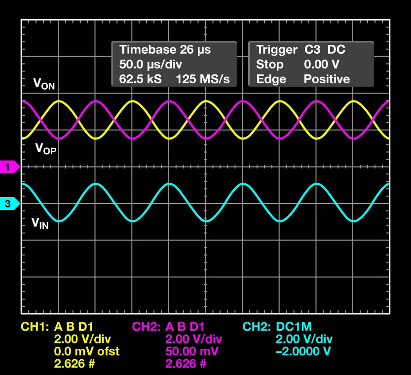
Jitter refers to the short-term variations in the timing of signal edges, which can accumulate and close the eye diagram in high-speed links. It arises from sources like power supply noise, crosstalk, and reflections in PCB traces. Deterministic jitter stems from repeatable causes such as impedance mismatches, while random jitter comes from thermal noise. In differential signaling, intra-pair skew exacerbates jitter, leading to timing errors at the receiver. PCB layout design plays a pivotal role in controlling these effects through careful routing and stackup planning. Effective jitter reduction preserves margins for eye height and width, critical for signal integrity.
Key PCB Layout Techniques for Differential Signaling
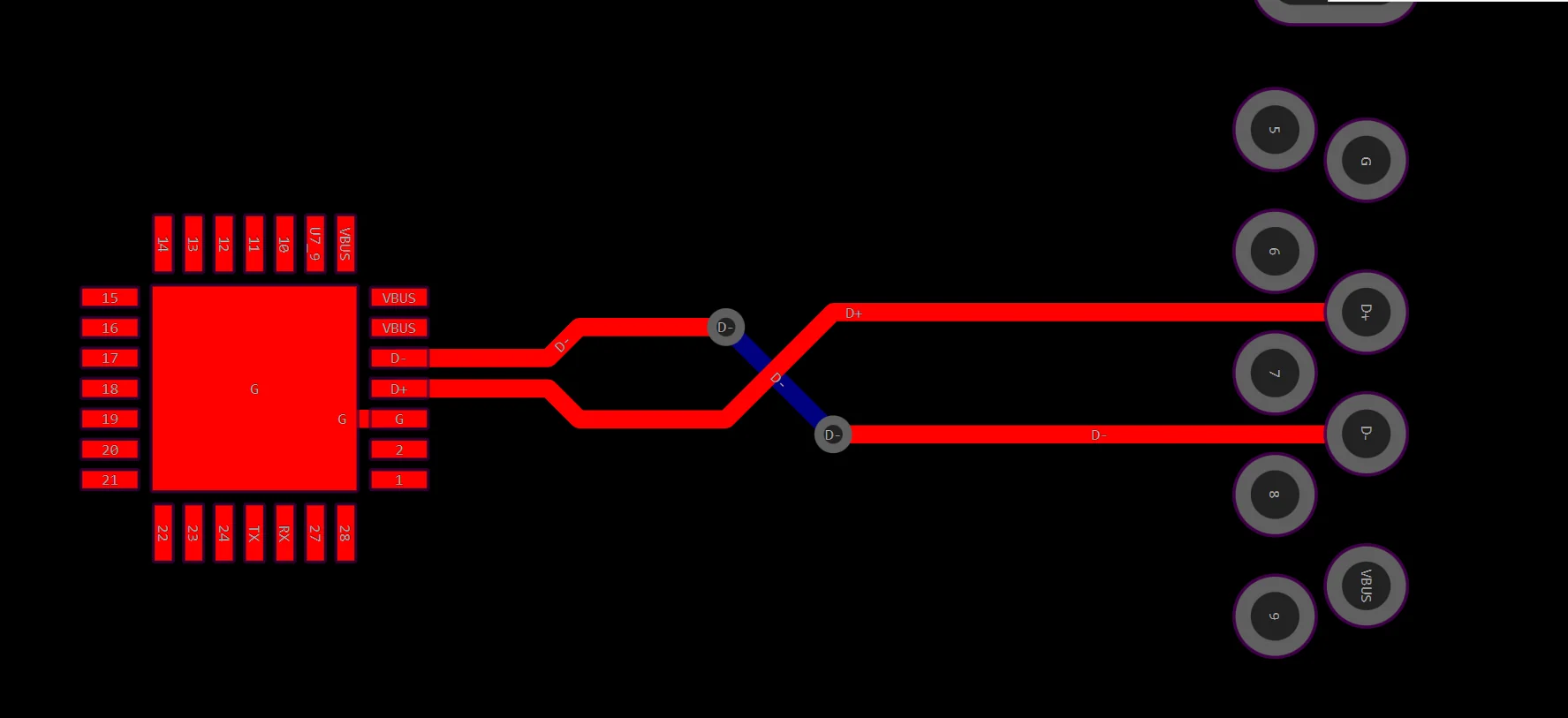
Routing differential pairs requires maintaining consistent trace width, spacing, and length to achieve controlled differential impedance, typically around 100 ohms. Pairs should remain coupled throughout their length, with spacing three times the trace width to minimize crosstalk from adjacent signals. Avoid routing pairs across plane splits or layer changes without backdrilling vias to prevent stubs that introduce reflections. Symmetric routing ensures equal propagation delays, reducing skew within the pair. Reference planes adjacent to signal layers provide a low-inductance return path. These PCB design guidelines form the foundation for robust signal integrity.
IPC-2221 provides essential guidance on trace geometries and spacing for controlled impedance in printed board design. Designers apply these principles to verify simulations before fabrication.
Strategies for Jitter Reduction in PCB Layout Design
To reduce jitter, implement length matching for differential pairs with tolerances under a few mils, depending on data rates. Use serpentine meanders for tuning, ensuring smooth bends to avoid impedance discontinuities. Solid ground planes under pairs distribute return currents evenly, minimizing loop inductance. Decoupling capacitors placed near drivers suppress power-related jitter. Minimize via count and use blind or buried vias where possible to shorten signal paths. These techniques collectively enhance timing stability in high-speed environments.
Crosstalk mitigation involves orthogonal routing of adjacent layers and sufficient inter-pair spacing. Pre-emphasis at transmitters can compensate for channel losses, but PCB layout must support clean propagation.
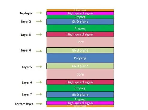
Optimizing Stackup and Reference Planes for Signal Integrity
A well-planned layer stackup is vital for differential signaling performance. Position signal layers between ground planes to confine fields and reduce radiation. Symmetric stackups prevent warpage and maintain consistent dielectric thickness. For multi-layer boards, dedicate inner layers to high-speed pairs with dedicated reference planes. Avoid splitting planes under pairs to ensure continuous return paths. These PCB layout design choices directly impact jitter by controlling characteristic impedance variations.
Via Management and Termination in Differential Pairs
Vias introduce discontinuities that generate reflections and jitter. Backdrill or use via-in-pad techniques to stub-minimize. For differential pairs, place vias symmetrically to preserve balance. Proper termination resistors at the receiver end match impedance and dampen reflections. Surface-mount terminations reduce parasitics compared to through-hole. Integrating these elements ensures optimal signal integrity across the board.
Power Integrity Considerations for Jitter Control
Power plane noise couples into signals, amplifying jitter in differential lines. Use dedicated power and ground planes with multiple vias for decoupling. Place low-ESR capacitors strategically near high-speed ICs. Plane stitching vias tie grounds together, providing low-impedance paths. These measures stabilize supplies and indirectly support jitter reduction. Engineers verify these through PDN simulations integrated with signal analysis.
IPC-6012 outlines qualification requirements for rigid printed boards, emphasizing performance under high-speed conditions.
Advanced Troubleshooting for Signal Integrity Issues
When jitter exceeds budgets, inspect eye diagrams from simulations or measurements. Common culprits include unmatched pair lengths or plane voids. Iterate stackup models to predict losses. Fabricate test coupons for validation. Collaborate with fabricators early for DFM checks. This systematic approach resolves issues before full production.
Conclusion
Mastering differential signaling and jitter reduction requires disciplined PCB layout design from stackup to routing. Key techniques like length matching, reference planes, and via optimization ensure signal integrity. Adhering to established PCB design guidelines minimizes risks in high-speed applications. Engineers who implement these practices achieve reliable performance and tighter timing margins. Continuous simulation and verification solidify these benefits. Ultimately, thoughtful layout elevates board quality and system longevity.
FAQs
Q1: What are the primary causes of jitter in differential signaling on PCBs?
A1: Jitter in differential signaling arises from impedance mismatches, crosstalk between pairs, and reflections from vias or plane splits. Power supply noise and dielectric variations also contribute. PCB layout design mitigates these by ensuring symmetric routing and solid references. Following signal integrity best practices keeps jitter within acceptable limits for high-speed data transmission.
Q2: How does length matching impact jitter reduction in PCB design?
A2: Length matching equalizes propagation delays in differential pairs, preventing intra-pair skew that amplifies jitter at the receiver. Use controlled meanders to tune without introducing discontinuities. This technique is essential for PCB design guidelines in gigabit interfaces. Simulations confirm compliance before layout finalization. Proper matching enhances eye opening and reduces bit errors.
Q3: What role do reference planes play in differential signaling signal integrity?
A3: Reference planes provide return paths for differential currents, minimizing loop inductance and EMI. Place them adjacent to signal layers for tight coupling. Avoid splits under pairs to prevent jitter from uneven returns. These elements are core to PCB layout design for high-speed performance. Solid planes improve overall signal integrity.
Q4: Why is controlled impedance critical for jitter reduction?
A4: Controlled impedance prevents reflections that cause deterministic jitter in differential traces. Maintain consistent width, spacing, and dielectric for target values. Verify with field solvers during design. This aligns with industry PCB design guidelines for reliable signaling. Deviations degrade timing margins significantly.
References
IPC-2221B — Generic Standard on Printed Board Design. IPC, 2012
IPC-6012E — Qualification and Performance Specification for Rigid Printed Boards. IPC, 2017
IPC-A-600K — Acceptability of Printed Boards. IPC, 2020


