










-
 03:34
03:34
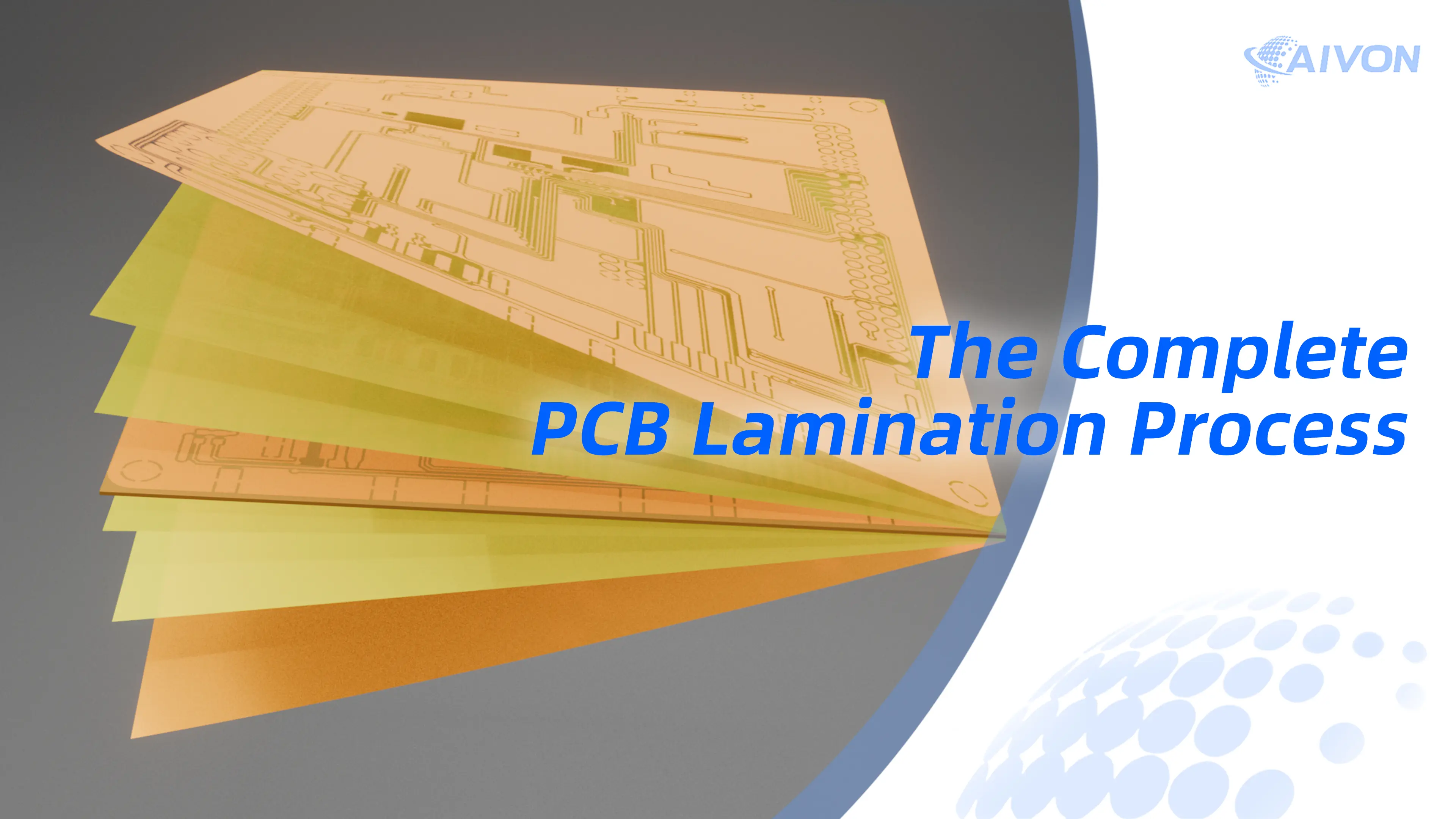
The Complete PCB Lamination Process: How Multilayer Boards Are Pressed Together
PCB lamination is a critical manufacturing process that bonds copper layers, cores, and prepregs into a single multilayer circuit board. This video provides an inside look at the lamination workflow, including inner layer surface treatment, cleanroom lay-up, high-pressure and high-temperature pressing, controlled cooling, alignment, and final trimming. It explains how factors such as material selection, resin flow, stack-up precision, and process control influence board thickness, layer integrity, warpage resistance, and long-term reliability. By understanding the lamination process, engineers and procurement teams can make better design and sourcing decisions for multilayer, HDI, prototype, and high-volume PCB applications.
-
 01:23
01:23
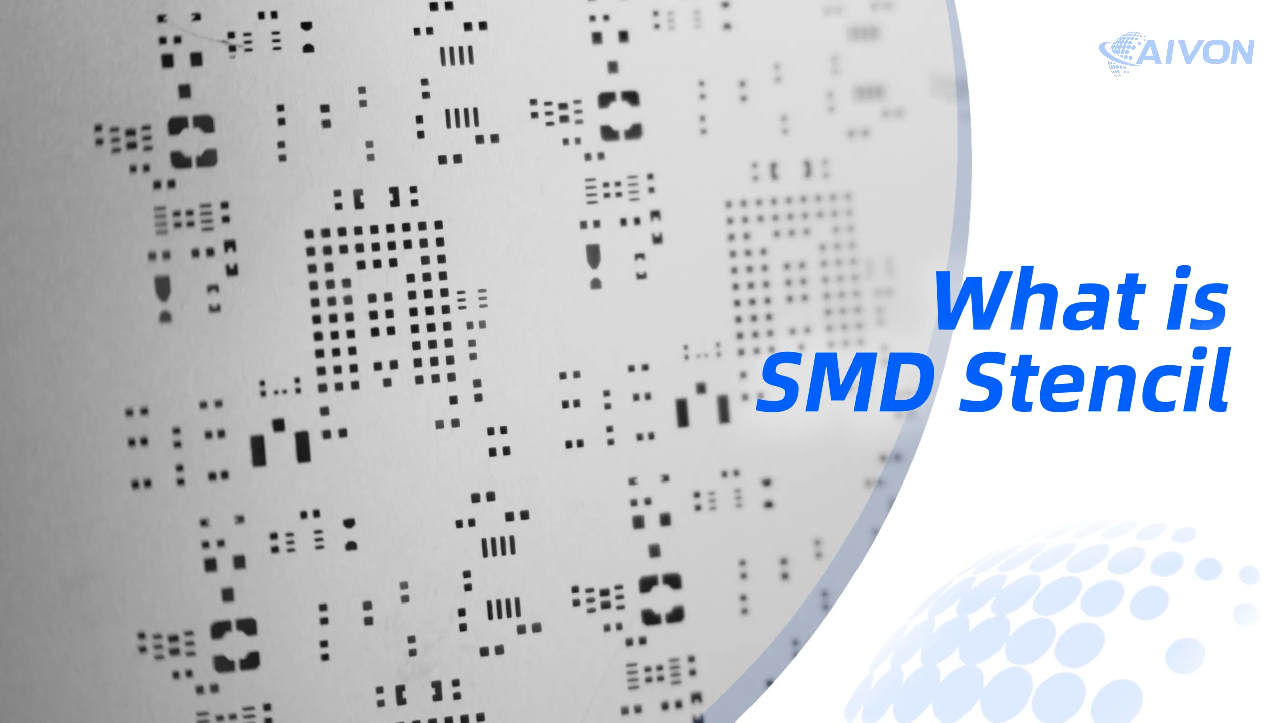
SMD Stencil Explained: How Precise Solder Paste Printing Works on PCBs
This video provides a detailed introduction to SMD stencils and their role in accurate solder paste printing during SMT assembly. It explains how laser-cut stainless-steel stencils precisely control solder paste deposition on PCB pads, ensuring reliable component placement and solder joint quality. The video highlights critical stencil parameters such as thickness, aperture design, surface smoothness, and paste release performance, especially for fine-pitch components like BGAs, QFNs, and miniature ICs. It also discusses optional electropolishing and nano-coating processes that improve paste release and reduce assembly defects. In addition, the video covers stencil applications from PCB prototyping to small-batch production and showcases our custom laser-cut stencil manufacturing capabilities in both framed and frameless formats.
-
 00:56
00:56
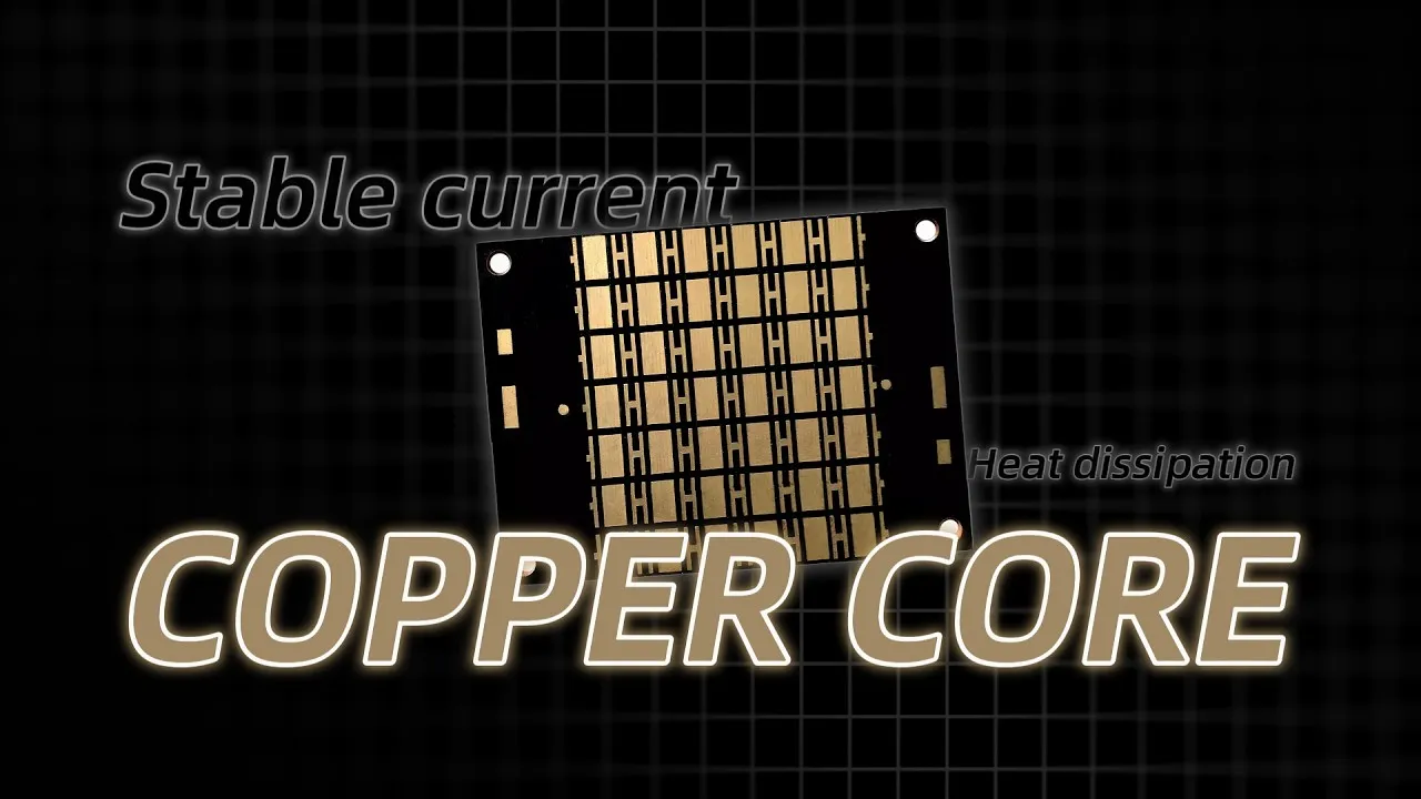
Copper Core PCB: High-Current and Power Handling Explained
This video provides a technical overview of CopperCore PCBs, also known as heavy copper PCBs, designed for high-current and high-power electronic applications. It explains how thick copper layers—up to 10 oz or more—deliver superior current-carrying capacity, enhanced heat dissipation, and improved mechanical durability compared to standard PCB constructions. The video also highlights how advanced etching and plating technologies maintain accurate trace geometries even with elevated copper weights. Key applications include power supplies, automotive electronics, industrial control systems, and renewable energy equipment where thermal stability and long-term reliability are critical. In addition, the video showcases our capabilities in multilayer heavy copper PCB fabrication, hybrid stack-ups, and integrated thermal management solutions.
-
 00:58
00:58
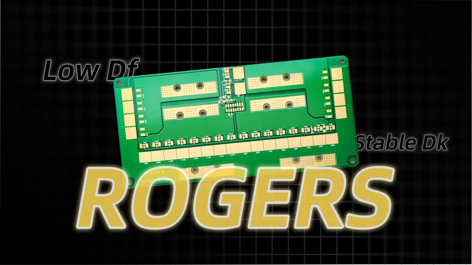
Rogers PCB: Low Loss, Stable Dk, High-Frequency Reliability
This video delivers a comprehensive engineering introduction to Rogers PCBs, highlighting their advantages in RF and microwave applications. It explains how Rogers materials provide low dielectric loss, stable dielectric constants, and superior thermal stability for maintaining excellent signal integrity and low insertion loss at high frequencies. The video also demonstrates why Rogers laminates outperform traditional FR4 in demanding environments requiring precise impedance control and long-term reliability. Key applications include 5G base stations, satellite communication systems, automotive radar, and medical imaging equipment. In addition, the video presents our manufacturing capabilities for multilayer RF, high-frequency, and high-speed Rogers PCB designs.
-
 01:01
01:01
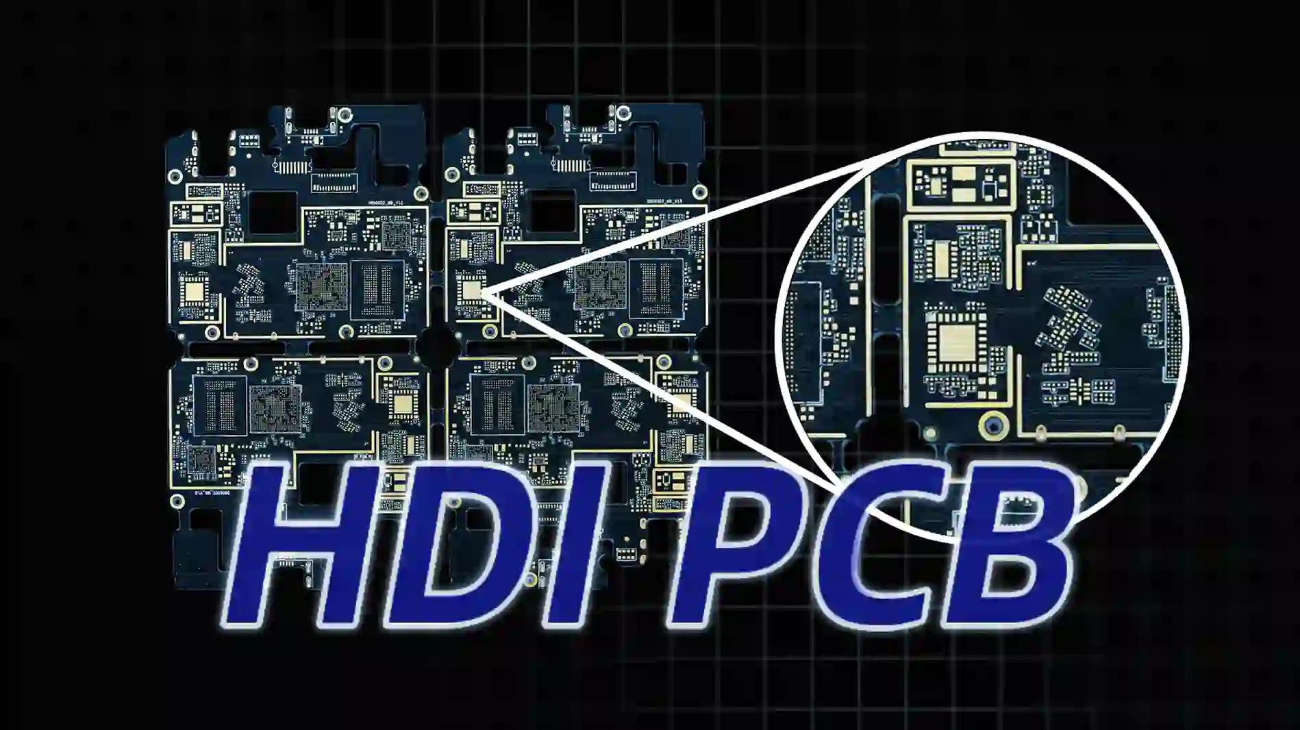
HDI PCB Fundamentals: Microvias, Density, and High-Speed Performance
This video provides a concise engineering introduction to HDI PCBs (high-density interconnect boards), explaining how microvias, fine traces, and thin dielectric layers increase circuit density and improve signal integrity in compact electronic designs. It covers key manufacturing technologies such as sequential lamination and laser drilling, along with performance benefits including faster signal transmission and reduced crosstalk. The video also highlights typical HDI PCB applications in smartphones, medical devices, tablets, and aerospace electronics, while presenting our fabrication capabilities such as up to 20-layer HDI structures, stacked and staggered microvias, controlled impedance routing, and advanced surface finishes.


