










Copper Core PCB: High-Current and Power Handling Explained
Key Moment
What This Video Covers
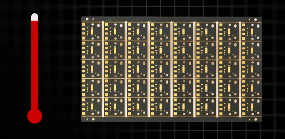
This video explains Copper Core PCBs - also known as heavy copper or thick copper boards - engineered for high-current and high-power applications. These boards use copper thicknesses up to 10 oz or more to maintain stable current flow while providing exceptional heat dissipation.
The core advantage is mechanical robustness and thermal performance. Copper Core designs reduce thermal stress, resist mechanical fatigue, and maintain consistent electrical performance in harsh environments where standard PCBs would fail. Advanced etching and plating processes ensure precise trace definition even at elevated copper weights.
You will learn why these boards are the preferred choice for power supplies, automotive electronics, industrial controls, renewable energy systems, and any application demanding extreme durability. The video also covers our capabilities in heavy multilayer Copper Core designs, hybrid stack-ups, and integrated thermal management solutions.
For immediate project support, explore our copper core PCB specifications or request a PCB quote. Additional guidance is available on our heavy copper PCB and power supply PCB pages.
Key Highlights
- Copper thicknesses up to 10 oz enable high-current carrying capacity and superior thermal dissipation in a single board.
- Advanced etching and plating processes maintain precise routing and trace integrity at heavy copper weights.
- Ideal for multilayer and hybrid stack-ups in power supplies, automotive electronics, and industrial control systems.
How Heavy Copper Layers Deliver Stable Current Capacity
Heavy copper layers in a Copper Core PCB fundamentally change current-handling behavior compared with standard 1 oz or 2 oz constructions. Current capacity scales with both copper cross-sectional area and allowable temperature rise. At 6–10 oz, a single trace can carry tens of amperes continuously while keeping temperature rise within typical 10–30 °C limits, provided the surrounding dielectric and copper plane structure dissipate the generated heat.
In production, fabricators must control copper thickness uniformity across the panel. Thickness variation greater than ±10 % at high ounce weights creates localized resistance hotspots that accelerate electromigration and early failure under sustained high current. Sequential plating and controlled etching compensate for this variation and keep final finished thickness within specification.
Designers benefit from placing high-current paths on outer layers when possible, because outer copper can be plated thicker more economically and offers better convection cooling. When inner-layer heavy copper is required, the stack-up must balance copper weight symmetrically to prevent board warpage during reflow and thermal cycling.
Failure to account for these factors commonly results in open traces or delamination after a few hundred power cycles. Proper Copper Core PCB layout therefore treats copper weight selection as a primary electrical and thermal design variable rather than a secondary material choice.
Manufacturing Precision in Etching and Plating Thick Copper
Etching heavy copper presents distinct process challenges. As copper thickness increases, lateral undercut becomes more pronounced because the etchant attacks the sidewalls for a longer time. At 8–10 oz, uncontrolled undercut can reduce final trace width by 20–30 % relative to the artwork, violating impedance and current-capacity targets. Fabricators therefore apply etch compensation factors and often use differential or sequential etch processes that remove copper in controlled stages.
Plating uniformity is equally critical. High-aspect-ratio vias and thick surface copper require optimized current-density distribution and additive chemistry to avoid plating voids or nodules. Voids in heavy-copper vias act as stress concentrators and frequently initiate barrel cracks during thermal cycling.
DFM best practice includes increasing minimum trace width and spacing with copper weight—typically 8–12 mil minimum for 4–6 oz and substantially larger for 10 oz—and communicating the intended final copper weight to the fabricator early so compensation can be applied correctly. Designs that ignore these process realities often experience open circuits after etching or intermittent failures after assembly.
Thermal Dissipation and Mechanical Robustness in Harsh Environments
The high thermal conductivity of thick copper planes and traces spreads heat laterally far more effectively than standard FR-4 constructions. In power-conversion and motor-drive applications, this reduces peak component temperatures and extends the life of both the PCB and attached semiconductors.
Mechanically, the increased copper volume raises the overall stiffness of the board and improves resistance to vibration-induced fatigue. However, the coefficient-of-thermal-expansion mismatch between heavy copper and the dielectric still exists. Repeated thermal cycling can therefore generate shear stresses at via interfaces and copper–dielectric boundaries. Balanced copper distribution, filled vias, and appropriate prepreg selection mitigate these stresses.
Observed field failures frequently involve cracked vias or lifted pads in regions of high copper density that experience rapid temperature swings. Copper Core PCB designs that incorporate thermal-relief patterns only where necessary, maintain copper balance, and specify appropriate glass-transition-temperature materials demonstrate markedly higher reliability under the same conditions.
Design for Manufacturability Rules for Multilayer Copper Core Stack-Ups
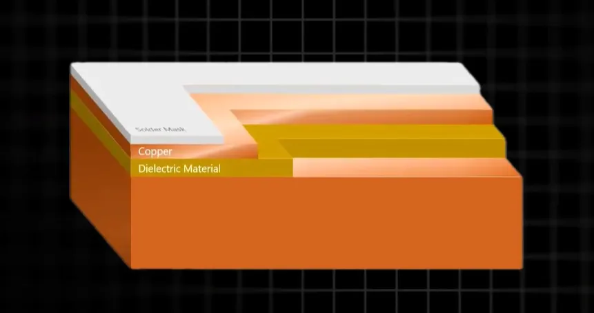
Hybrid stack-ups that combine standard-weight signal layers with heavy-copper power layers require careful sequencing of lamination and plating cycles. The fabricator must ensure that the thick copper does not create excessive topography that prevents reliable bonding of subsequent layers.
Recommended practices include specifying finished copper weight rather than starting foil weight, allowing adequate annular ring on heavy-copper vias, and avoiding fine-pitch features on the same layer as high-ounce copper. When mixed copper weights are mandatory, staggered via structures and selective plating reduce process risk.
Boards that violate these guidelines commonly exhibit registration errors, incomplete plating, or delamination after reflow. Early collaboration with the manufacturer on stack-up drawings and process capability data prevents these issues and yields a manufacturable design on the first iteration.
Key Application Sectors Relying on Copper Core Technology
Copper Core PCBs are routinely specified in switch-mode power supplies, electric-vehicle power distribution modules, industrial motor drives, solar and wind inverter stages, and high-power LED drivers. In each case the combination of high continuous current, elevated ambient temperature, and mechanical vibration makes standard copper weights inadequate.
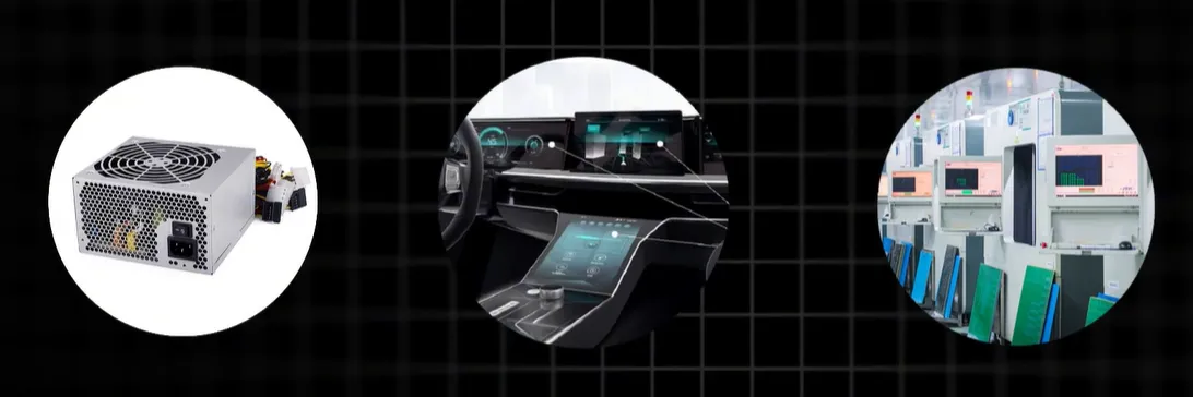
The video illustrates representative constructions used in these sectors and highlights how multilayer heavy-copper boards integrate power and control circuitry on a single reliable platform.
| Copper Weight | Typical Continuous Current Capacity (10 mil trace, 20 °C rise) | Relative Thermal Spreading | Common Process Notes |
|---|---|---|---|
| 1 oz | ~1.0–1.5 A | Baseline | Standard etching |
| 3 oz | ~3–4 A | Moderate improvement | Moderate undercut compensation |
| 6 oz | ~6–8 A | Significant | Sequential etch recommended |
| 10 oz | ~10–14 A | Highest | Specialized plating & compensation essential |
FAQ
Q1: How thick is copper typically in CopperCore PCBs for high-power applications?
A1: CopperCore PCBs commonly use 3–10 oz copper, with some designs exceeding 10 oz for extreme current loads.
Q2: What advantages do CopperCore PCBs offer over standard FR4 boards in high-current designs?
A2: They provide significantly better heat dissipation, higher current capacity, greater mechanical strength, and improved long-term reliability under thermal cycling.
Q3: Which industries require CopperCore PCB technology most often?
A3: Power supplies, automotive electronics, industrial automation, renewable energy inverters, and any system with high power density or harsh operating conditions.
Q4: What etching challenges arise when fabricating Copper Core PCBs above 4 oz?
A4: Increased lateral undercut reduces final trace width if not compensated. Specialized multi-stage etching, artwork compensation, and tighter process control are required to maintain dimensional accuracy and current-carrying capacity.
Q5: How should designers address via reliability in multilayer Copper Core constructions?
A5: Specify adequate annular rings, consider filled or capped vias, balance copper distribution across layers, and verify the fabricator's plating capability for the target aspect ratio and copper weight. These steps reduce the risk of barrel cracks during thermal cycling.
This is a CopperCore PCB — a heavy copper board designed for high-current and power electronics.
Built with copper thicknesses up to 10 oz or more, it enables stable current flow and superior heat dissipation.
Its biggest advantage is robustness: CopperCore materials handle extreme power loads, reduce thermal stress, and extend product lifespan.
They also improve reliability in demanding environments, ensuring mechanical strength and consistent performance where standard PCBs would fail.
And with advanced etching and plating processes, CopperCore boards support precise routing even at high copper weights.
You'll find CopperCore PCBs in power supplies, automotive electronics, industrial controls, renewable energy systems, and any product where durability and power handling are critical.
We support heavy multilayer CopperCore designs, hybrid stack-ups, and advanced thermal management solutions.
Feel free to explore specifications, datasheets, and stack-up guidelines on our platform whenever you need them.





