 00:56
00:56
Heavy-Copper PCB
Heavy copper PCBs represent a specialized category of printed circuit boards designed to handle high current loads and improve thermal management in demanding applications. These boards feature copper traces and planes with thicknesses typically exceeding 3 ounces per square foot, often ranging from 4 to 20 ounces or more, which enhances their ability to conduct electricity efficiently while dissipating heat effectively. For engineers and designers searching for heavy copper PCB solutions, this tag compiles essential resources that address key challenges in power electronics, such as reducing voltage drops, minimizing thermal hotspots, and ensuring long-term reliability in harsh environments. Understanding the advantages of heavy copper PCBs is crucial for projects involving high power density, including electric vehicle chargers, renewable energy inverters, industrial motor drives, and aerospace systems. By incorporating thicker copper layers, these boards can support currents up to several hundred amperes without the need for additional heat sinks or complex cooling mechanisms, leading to more compact and cost-effective designs. Practical insights from our articles cover fabrication techniques like copper plating and etching processes, which help avoid common pitfalls such as delamination or uneven thickness. Best practices include selecting appropriate base materials like FR4 or polyimide for thermal stability, and optimizing trace widths to balance current capacity with board real estate. For those integrating heavy copper PCBs into prototypes or production runs, considerations around impedance control and signal integrity become vital, especially in mixed-signal designs. Our collection of articles delves into these topics, offering guidance on simulation tools for thermal modeling and compliance with standards like IPC-2152 for current-carrying capacity. Whether you are troubleshooting thermal issues or scaling up for high-volume manufacturing, the content here provides actionable strategies to enhance performance and reliability. Browsing through related posts can offer deeper dives into case studies and emerging trends in heavy copper technology, helping you refine your approach to complex electronic systems.
Video Guide

Technical Articles
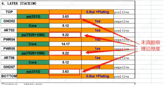
How PCB Copper Thickness Affects Current, Heat, and Strength
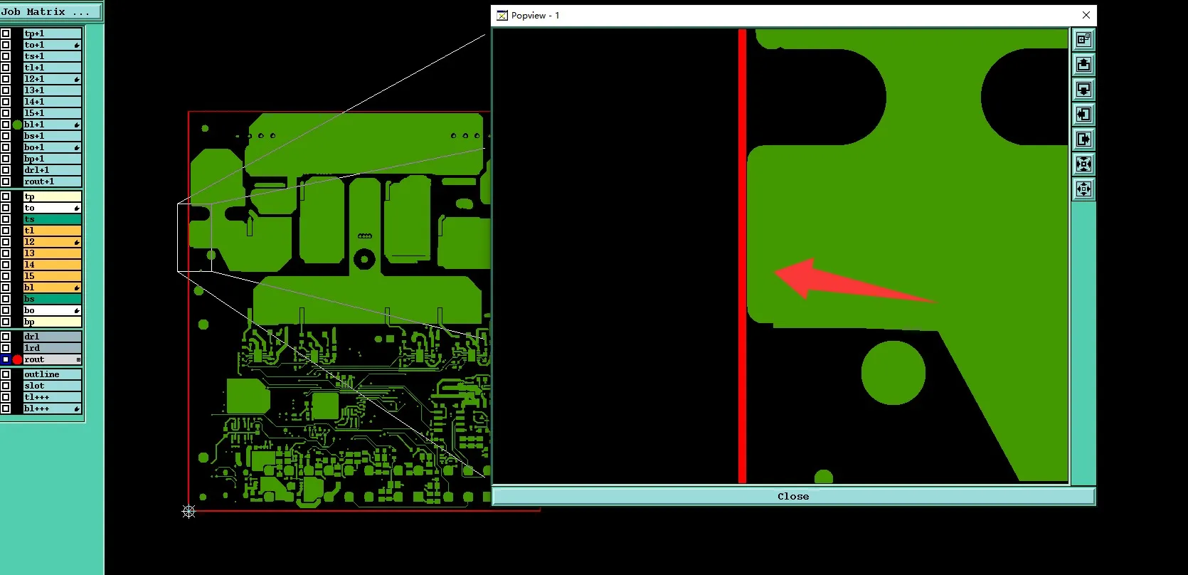
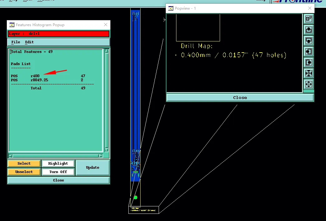
6-Layer 2oz Heavy Copper FR-4 PCB Engineering Review: Edge Clearance, Hole Attribute Conflicts and Silkscreen Overlap Case
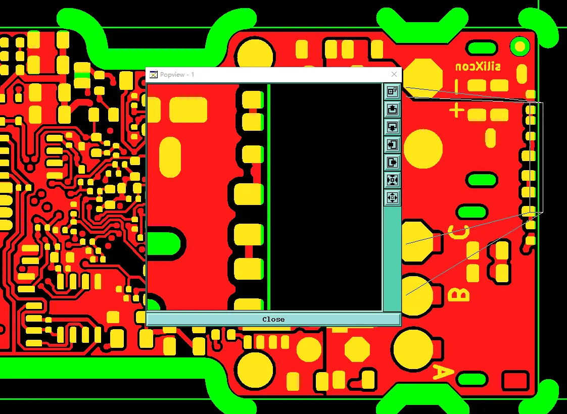
2-Layer 4mm Thick PCB DFM Case: Panelization, Via Tenting & Tooling Hole Challenges
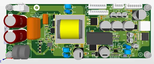
4-Layer 3oz Heavy Copper PCB DFM Case: V-CUT Pad Damage Risk and Plated Slot Clarifications
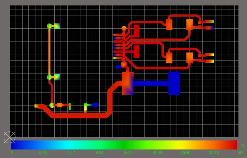
Thick Copper PCBs: Enabling Compact and Efficient DC DC Converters
Layer Thickness Matters: Optimizing Your PCB for Current Capacity and Thermal Management
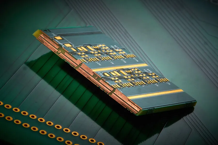
DIY Power Supply? Why a Thick PCB is Your Best Friend

Choosing Circuit Breakers, Contactors and Wires by Motor Power
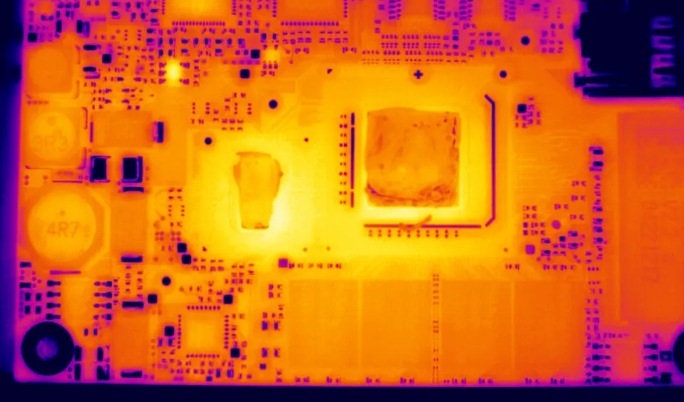
Thermal Runaway: Managing Heat Dissipation in Maximum Sized PCBs
Understanding Power Supply PCB Certifications and Standards
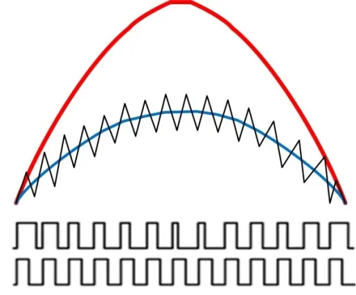
PFC BCM vs CCM Modes Explained: Power Factor Correction in Power Supplies
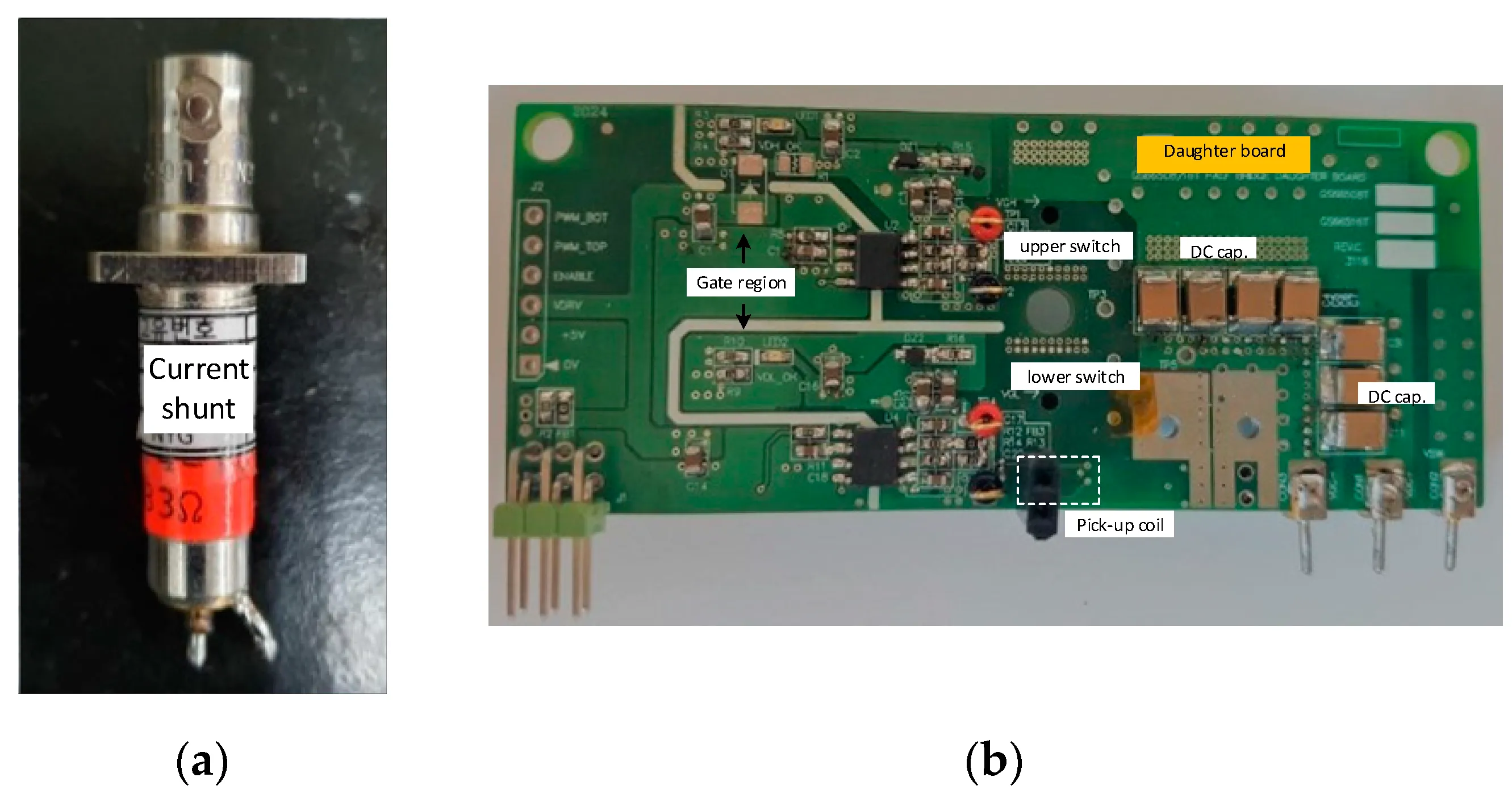
Isolated Current Sensors: Design Considerations for High Voltage PCB Applications

Electrical Advantages of SiC Power Devices
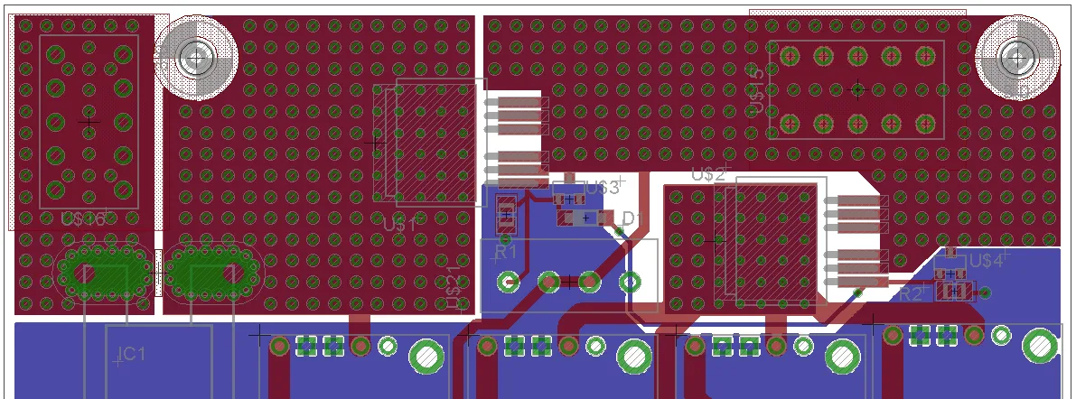
Taming High Currents: Advanced PCB Power Distribution Techniques for Power Electronics
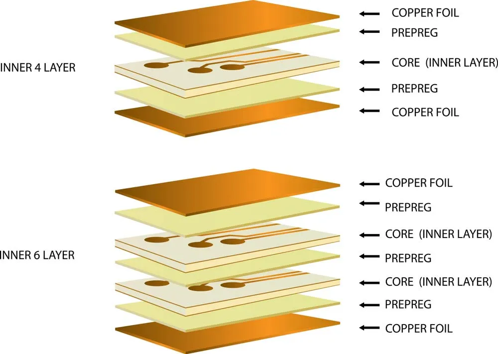
Understanding Copper Weight in PCB Stack Up: A Detailed Guide

China IGBT Manufacturers: Capacity Expansion & PCB Design Impact
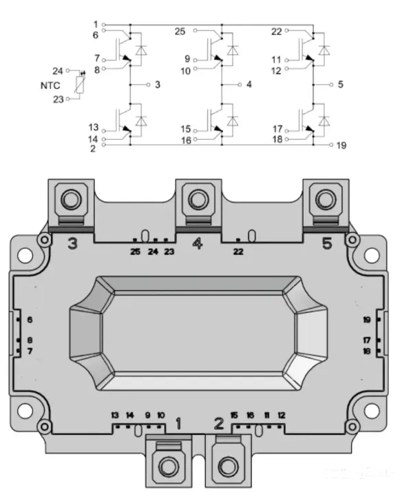
Common Automotive IGBT Module Package Types: Technologies, Applications, and PCB Integration in New Energy Vehicles

Silicon Carbide in Modern Power Electronics: PCB Design and Manufacturing Considerations
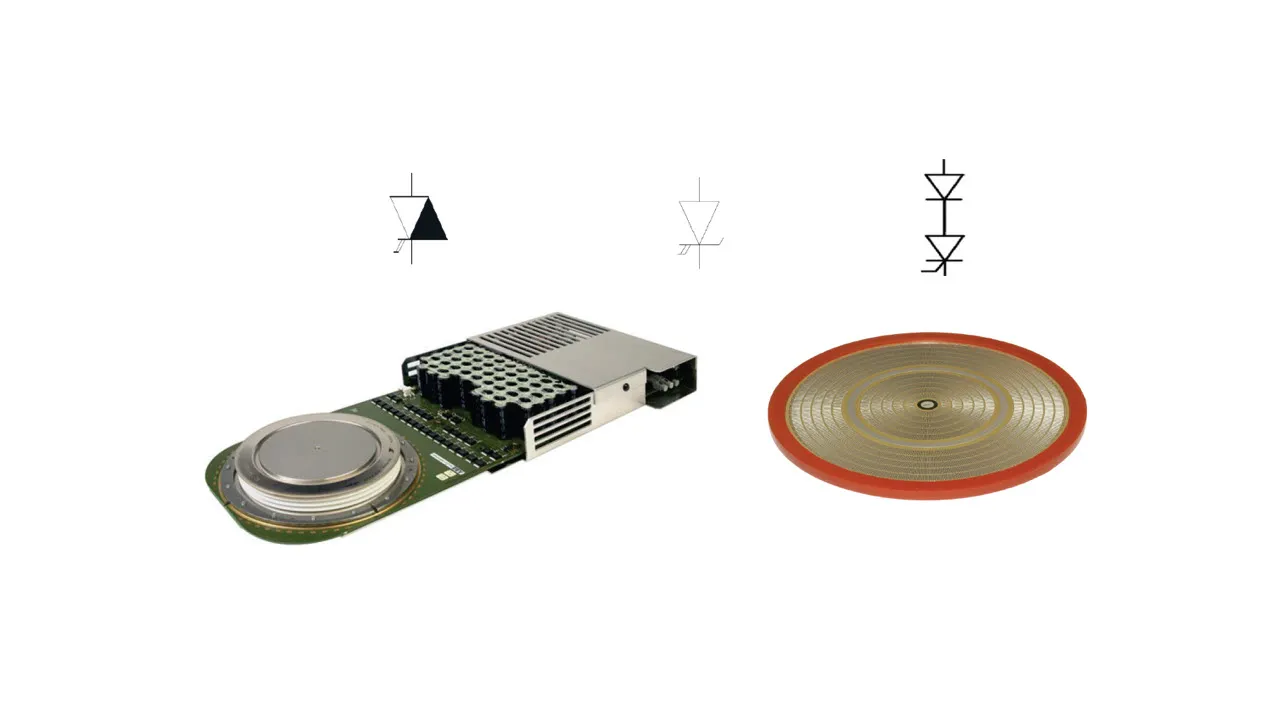
IGCT Overview: Integrated Gate-Commutated Thyristor Technology & Applications