Introduction
Building a DIY power supply is one of the most rewarding projects for electronic hobbyists. It powers everything from LED strips to small motors, but handling high currents often leads to overheated traces, voltage drops, and failed prototypes. A thick PCB changes that equation entirely by providing robust current handling right from the start. Hobbyists quickly discover that standard thin copper layers struggle with power demands, leading to frustrating redesigns. Choosing a thick PCB for hobby projects ensures reliability without complex workarounds. This article explores why thick PCBs are essential for high-current applications like DIY power supplies and shares practical tips for beginners.
What Is a Thick PCB and Why It Matters for DIY Power Supplies
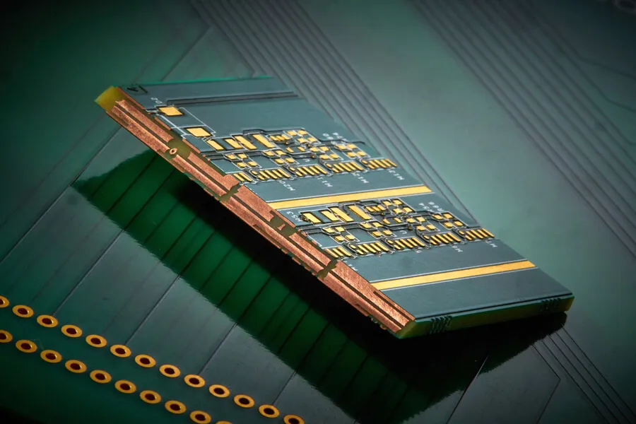
A thick PCB typically refers to boards with heavier copper weights, such as 2 ounces per square foot or more, compared to the standard 1 ounce. This extra copper thickness allows traces and planes to carry significantly more current without excessive heating. For hobbyists building DIY power supply PCBs, this means delivering stable voltages to loads like amplifiers or chargers without meltdown risks. Standard PCBs limit current to low levels, forcing wide traces that eat up board space and complicate layouts. Thick copper solves these issues, making high current PCB designs accessible even for beginners. In power supplies, where rectifiers, regulators, and output stages demand robust paths, a thick PCB prevents common failures and boosts project success rates.
The relevance grows as hobby projects scale up. A simple 5V supply for USB devices might work on thin copper, but stepping to 12V at several amps reveals limitations fast. Thick PCBs align with industry needs for thermal management and electrical performance, ensuring your build lasts through testing and daily use. Hobbyists appreciate how this choice simplifies troubleshooting, as failures shift from PCB issues to component selection.
The Technical Principles Behind Thick Copper PCBs
Copper thickness directly impacts a PCB's ability to handle current, governed by principles of electrical resistance and thermal dissipation. Thicker copper reduces resistance per unit length, minimizing voltage drops across power traces. This keeps output voltages stable under load, critical for DIY power supplies where even small drops affect performance. Heat generation follows Joule heating, where I squared R losses concentrate in thin traces, risking delamination or charring. IPC-2152 provides guidelines on current-carrying capacity, factoring in trace width, thickness, and temperature rise to predict safe limits.
Thermal conductivity plays a key role too. Thick copper spreads heat more effectively across the board, acting as a built-in heatsink for power components. In multilayer boards, inner layers with thick copper enhance vertical heat transfer when paired with vias. Mechanical strength increases as well, resisting warpage from soldering or mechanical stress. These mechanisms make thick PCB advantages for hobbyists clear: reliable operation without added cooling hardware.
Voltage drop calculations become straightforward with thicker layers. For a given current, thicker copper requires narrower traces, freeing space for other circuits. This efficiency shines in compact DIY designs, where board real estate is precious.
Advantages of Thick PCBs for Hobbyists Building High-Current Projects
One primary benefit is superior current capacity, allowing hobbyists to power demanding loads like bench supplies or motor drivers. Thick copper handles amps where standard boards falter, reducing the need for external bus bars or wires. This streamlines assembly, as everything stays on the PCB. Heat management improves dramatically, with lower temperature rises enabling closer component spacing and simpler enclosures.
Mechanical robustness stands out for hands-on projects. Thicker boards withstand bending, drilling errors, or mounting stresses better than fragile standards. For DIY power supply PCBs, this means durable prototypes that survive bench testing. Cost savings emerge over time, as fewer layers suffice for power distribution, and failures drop.
Fabrication tolerance improves with thick copper in select areas, like power planes. Hobbyists gain compact designs without sacrificing performance, ideal for easy PCB design for high power. Overall, these perks turn challenging high-current builds into straightforward successes.
Best Practices for Designing a DIY Power Supply PCB with Thick Copper
Start by identifying high-current paths: input rectification, filtering capacitors, regulators, and outputs. Assign thick copper, say 2oz or more, to these traces and use copper pours for planes. Keep traces as wide as possible within space constraints, following general rules for low resistance. Incorporate thermal vias under hot components to wick heat to inner layers or the opposite side.
Layer stackup matters; a 2-layer board with thick outer copper works for most hobby supplies. Ensure adequate spacing to prevent arcing at higher voltages, typically following IPC-6012 performance specs. Use ground planes on unused areas to aid shielding and heat spreading. For beginners, sketch power flow first, then route signals away from noisy power lines.
Soldering thick copper requires care: preheat boards to avoid cracking, and use flux generously for reliable joints. Test current limits gradually with dummy loads to verify performance. These steps make high current PCB for beginners reliable and repeatable.

Common Pitfalls and How to Avoid Them in Thick PCB Designs
Thicker copper etches differently, with undercuts larger due to aspect ratios, potentially narrowing traces. Specify conservative widths in your design files to compensate. Vias for thick layers need plating adjustments; use larger diameters or filled vias for current paths. Warpage risk rises from uneven copper distribution, so balance layers symmetrically.
Component mounting challenges arise with rigid thick boards; flexible leads help. Overlooking thermal expansion can stress solder joints, so align coefficients where possible. Beginners often ignore fab limits, so confirm copper weights upfront. Addressing these keeps your thick PCB for hobby projects smooth.
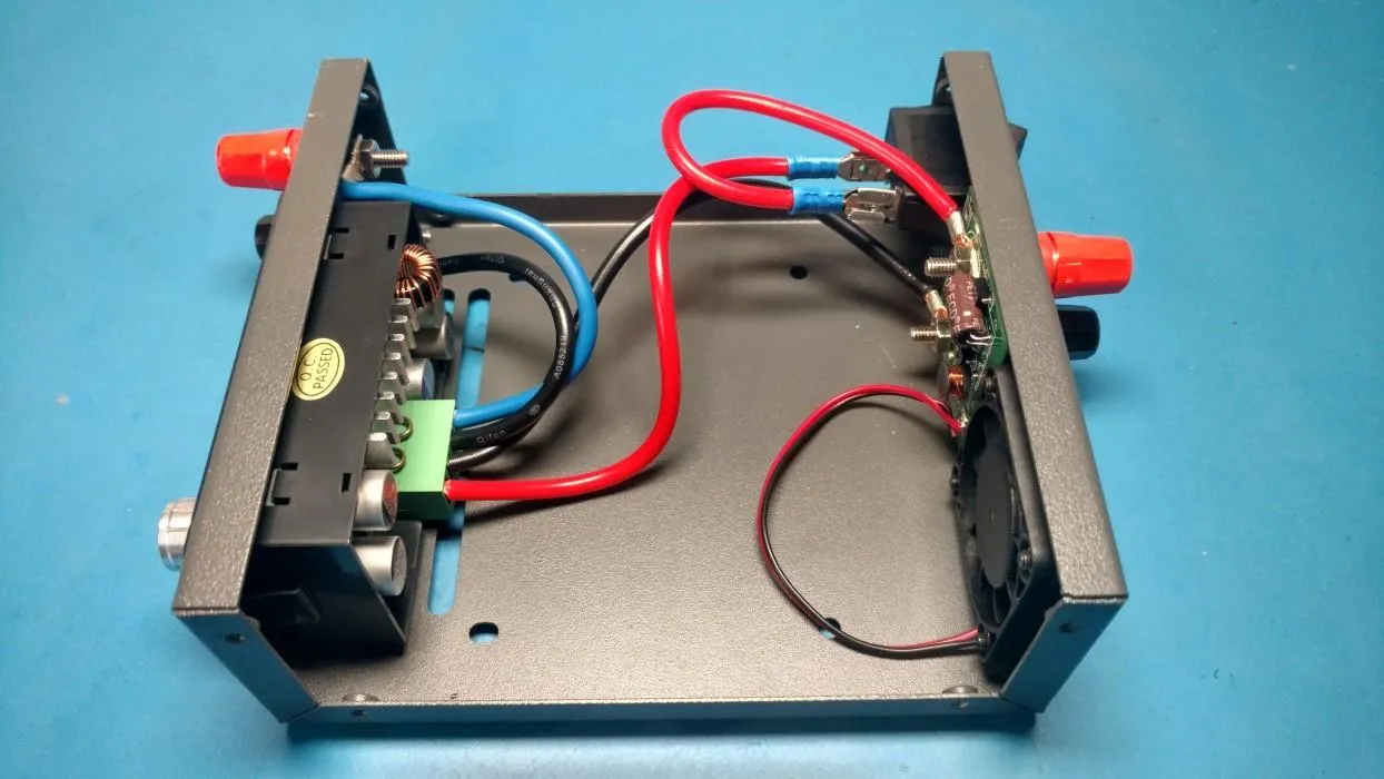
Case Study: Building a Simple 12V 10A Bench Power Supply
Consider a hobbyist's adjustable 12V supply for testing circuits. Using a thick PCB with 2oz copper on power traces, the rectifier bridge and inductor paths stayed cool under full load. Standard 1oz attempts overheated at 5A, forcing redesigns. Wide output pours distributed current evenly, with thermal vias under the regulator IC.
Assembly used through-hole components for easy soldering, paired with SMD caps for compactness. Voltage sensing traces ran parallel but separated to avoid interference. Testing showed under 0.1V drop at 10A, far better than wire hacks. This build highlights thick PCB advantages for hobbyists in real-world power delivery.
Conclusion
Thick PCBs transform DIY power supply projects from risky experiments to dependable tools. Their ability to manage high currents, dissipate heat, and provide mechanical strength addresses core hobbyist pain points. By integrating thick copper thoughtfully, beginners achieve professional results without advanced skills. Follow best practices like wide traces and thermal management for success. Embrace thick PCBs, and watch your high-power creations thrive reliably.
FAQs
Q1: What makes a thick PCB ideal for high current PCB for beginners in DIY power supplies?
A1: Thick PCBs feature heavier copper layers that carry more current with less heat buildup, perfect for novice builds. They reduce voltage drops and simplify layouts by allowing narrower traces for the same ampacity. Hobbyists avoid common failures like melted traces, making prototyping faster. Standards like IPC-2152 guide safe designs, ensuring reliability from the first run.
Q2: How do thick PCB advantages for hobbyists improve DIY power supply performance?
A2: Advantages include better thermal spreading, mechanical durability, and efficient power distribution. Heat stays low, extending component life in power stages. Compact designs fit enclosures easily, ideal for bench use. Beginners gain confidence with stable outputs under load, skipping bulky wiring.
Q3: What are easy PCB design tips for high power using thick copper?
A3: Prioritize power paths with thick copper pours and wide traces. Add thermal vias and ground planes for cooling. Separate signal lines from power to minimize noise. Verify fab specs for copper weight. This approach yields robust DIY power supply PCBs without complexity.
Q4: Can hobbyists use thick PCBs for all projects, or just power supplies?
A4: Thick PCBs excel in high-current needs like power supplies but add cost and etching challenges elsewhere. Reserve them for power sections, using standard copper for signals. This hybrid maximizes thick PCB for hobby projects benefits while keeping designs affordable and manufacturable.
References
IPC-2152 — Current-Carrying Capacity in Printed Board Design. IPC.
IPC-2221 — Generic Standard on Printed Board Design. IPC.
IPC-6012E — Qualification and Performance Specification for Rigid Printed Boards. IPC, 2017.


