










KiCad Hub
KiCad Hub: Guides, Tips, and Best Practices
Featured Blog

What Is KiCad? A Complete Introduction to Open Source PCB Design Software
Learn what KiCad is, its core features for schematic design, PCB layout, 3D visualization, and manufacturing output. Discover why engineers choose this free open-source tool and how to move from design to professional PCB fabrication.
Latest Blogs
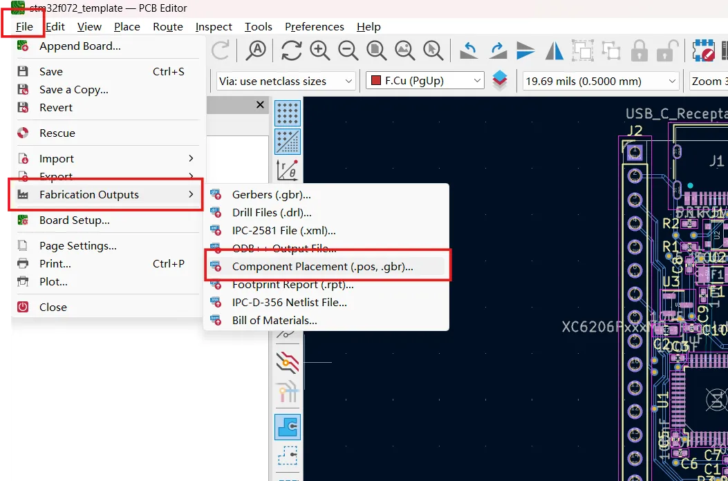
Generating Pick-and-Place Files in KiCad: Complete SMT Assembly Guide
Learn how to generate accurate pick-and-place (centroid/position) files in KiCad for SMT assembly. Covers export workflow, file contents, common issues, verification tips, and manufacturer preparation.
Common KiCad PCB Manufacturing Problems and How to Fix Them
Discover the most common KiCad PCB manufacturing problems—incorrect footprints, missing Gerbers, design rule violations, and assembly issues—plus practical fixes to improve DFM and avoid costly respins.
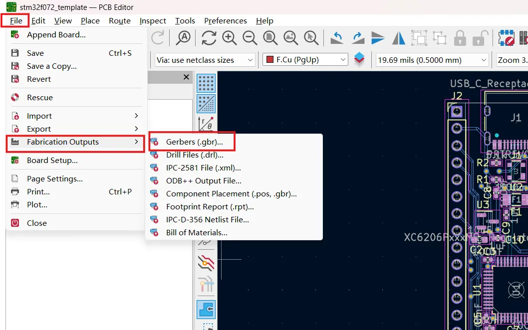
How to Export Gerber Files from KiCad for PCB Manufacturing
Learn how to correctly export Gerber and drill files from KiCad for PCB manufacturing. Covers preparation, layer selection, common export mistakes, verification steps, and streamlined workflows for production-ready data.
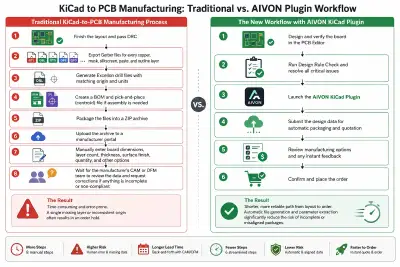
How to Order PCBs Directly from KiCad: Complete Manufacturing Workflow
Learn how to order PCBs directly from KiCad with a complete manufacturing workflow. Compare traditional export steps vs the integrated plugin process, required files, and how to go from design to production faster.
KiCad Plugin vs Manual Gerber Upload: Which PCB Ordering Workflow Is Better?
Compare KiCad plugin vs manual Gerber upload for PCB ordering. Explore advantages, limitations, and which workflow is better for beginners or professionals to reduce errors and speed up manufacturing.
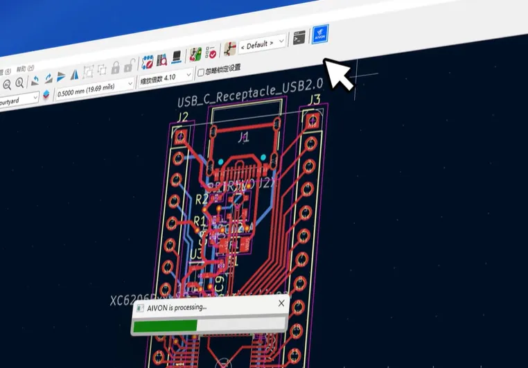
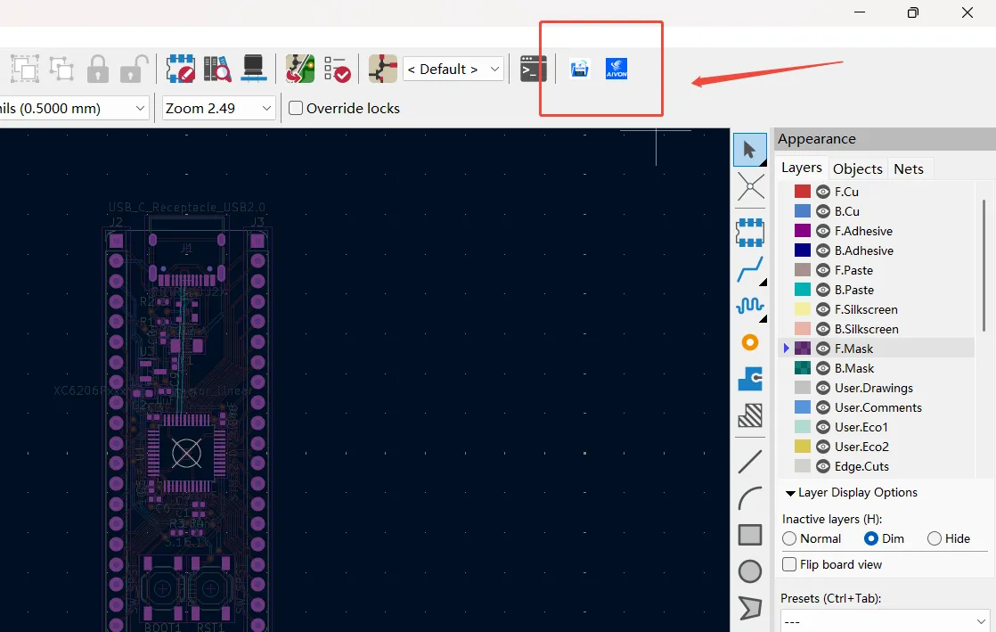
How to Install and Use AIVON KiCad Plugin for PCB Ordering
Step-by-step guide to install the AIVON KiCad plugin, get instant PCB quotes, and skip manual Gerber uploads. Learn the complete workflow from design to manufacturing.

What Is AIVON KiCad Plugin? Simplify PCB Ordering from KiCad
Learn how the AIVON KiCad Plugin simplifies PCB ordering. Generate Gerbers, BOM & PnP files and submit to manufacturing without leaving KiCad. Faster prototypes, fewer file errors.
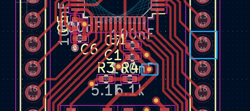
Via Design Guidelines for KiCad PCBs: Types, Rules and Manufacturing Considerations
Learn practical via design guidelines for KiCad PCBs. Cover via types (through-hole, blind, buried, microvias), size rules, clearances, placement best practices, and manufacturing limits to create reliable boards.
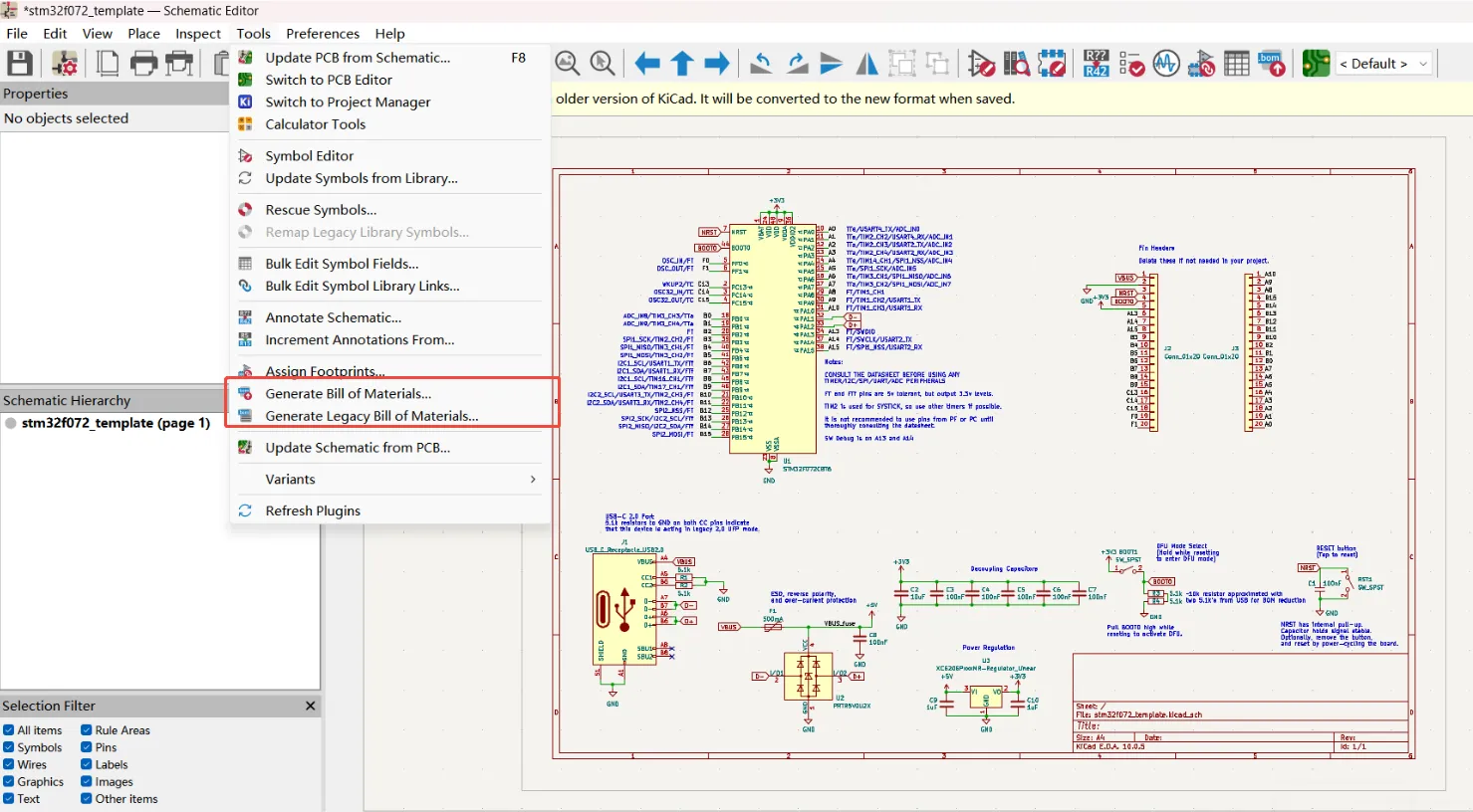
Exporting BOM Files from KiCad: Complete Guide for PCB Assembly
Learn how to export accurate BOM files from KiCad for PCB assembly. This guide covers required fields, manufacturer part numbers, file formats, common errors and a checklist to ensure smooth PCBA production.
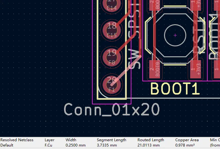
Choosing the Right Trace Width in KiCad: PCB Design Rules and Guidelines
Learn how to set optimal PCB trace width in KiCad. Covers net classes, current capacity, signal integrity, copper thickness, and manufacturing limits for reliable boards.
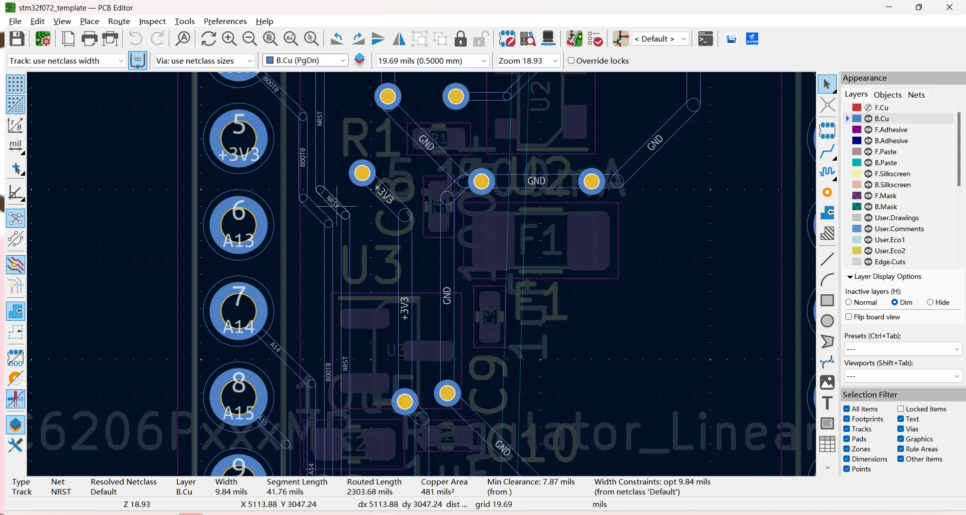
Working with Copper Zones in KiCad: Ground Planes and Design Guidelines
Learn how to create and manage copper zones in KiCad for reliable ground planes. This guide covers zone settings, thermal reliefs, clearance rules, common fill problems and manufacturing tips to improve PCB performance and yield.
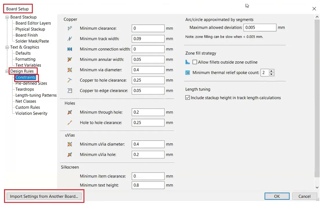
KiCad PCB Design Rules: How to Prepare Your Board for Manufacturing
Learn how to set KiCad PCB design rules for real manufacturing. This guide covers trace width, clearance, via size, common DFM issues, DRC checks and factory-oriented tips to ensure your board passes production review.


