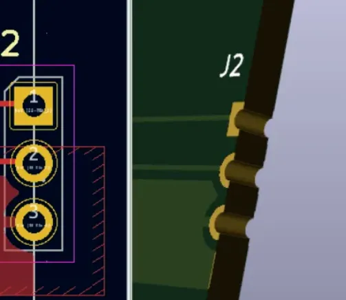
A board that passes every electrical check can still fail at the assembly house. The most common reason is a footprint that does not match the real component: pads too small, courtyard missing, silkscreen covering a pad, or polarity mark in the wrong place. The schematic looked perfect. The netlist was clean. Yet the physical parts cannot be soldered reliably.
This article explains what a footprint actually is in KiCad, how it relates to the schematic symbol, and the practical steps to create, edit, and manage footprints so they survive both design-rule checking and real manufacturing. You will learn how to avoid the footprint errors that force respins and how to build libraries that stay consistent across projects.
What Is a Footprint in PCB Design?
A footprint is the physical land pattern of a component on the PCB. It defines the copper pads, solder-mask openings, silkscreen outlines, courtyard, and (optionally) a 3D model. In KiCad the footprint is stored separately from the schematic symbol. The symbol describes the electrical pins; the footprint describes the physical geometry that the fabricator and the assembler will use.
Why footprints affect manufacturing quality is straightforward. The fabricator drills holes and etches copper according to the footprint pads. The assembler places parts according to the courtyard and polarity marks. If either is wrong, yield drops. Professional teams treat footprint accuracy as a design-rule requirement, not an afterthought.
Symbol vs Footprint in KiCad
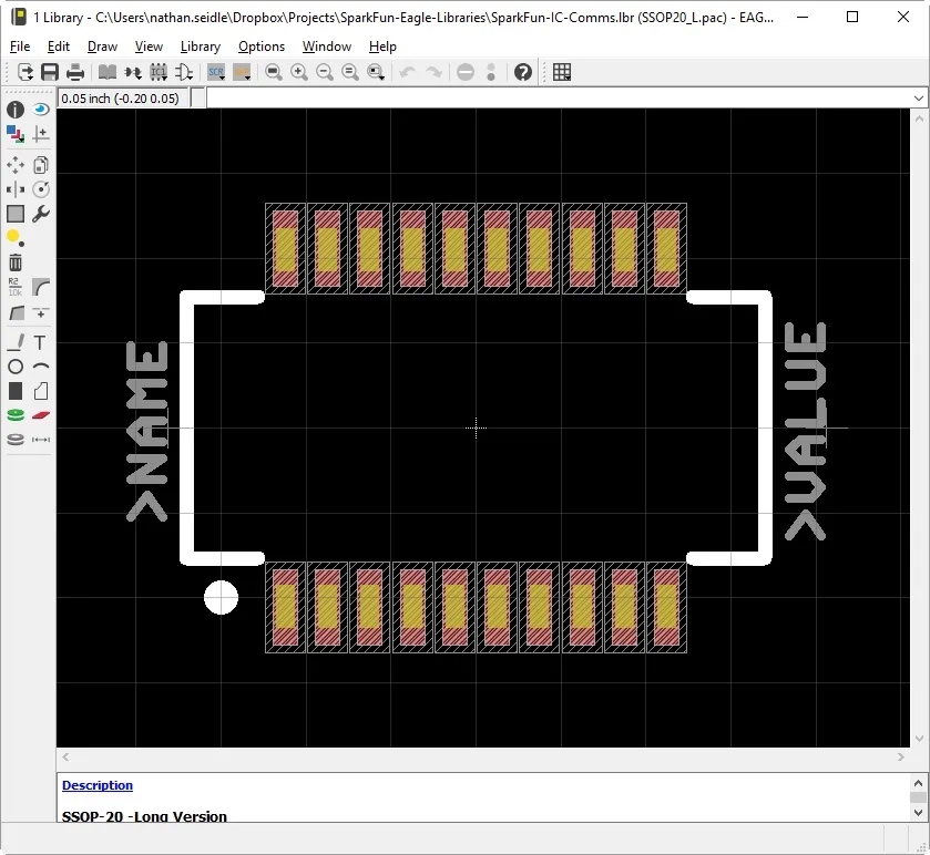
In KiCad the schematic symbol and the PCB footprint are linked but independent. The symbol lives in a symbol library and carries pin numbers, electrical types, and a footprint assignment field. The footprint lives in a footprint library and carries the geometric data.
When you place a symbol in the schematic, you assign (or confirm) its footprint. Later, when you update the PCB from the schematic, KiCad places the corresponding footprint on the board and connects the pads according to the pin mapping.
Practical guidance:
- Always verify the footprint field after placing a symbol.
- Prefer symbols that already have a trusted footprint association.
- Use the "Change Footprints" tool when you need to swap an entire series of parts.
Common mistake: assuming the default footprint is correct. Many official symbols point to generic footprints that do not match the exact package dimensions in the datasheet. Always open the footprint and compare it with the manufacturer's recommended land pattern before finalizing the design.
Manufacturing perspective: an incorrect pad size or missing thermal pad can cause tombstoning, open joints, or insufficient solder. These defects appear only after reflow and are expensive to rework.
Using KiCad Footprint Libraries
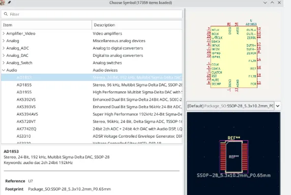
KiCad ships with a large set of standard libraries (Resistor_SMD, Capacitor_SMD, Package_SO, Package_QFP, etc.). These libraries are maintained by the community and cover most common packages.
Recommended workflow for selecting footprints:
- Open the Footprint Library Browser or use the footprint chooser from the schematic.
- Search by package name or keyword (e.g., "SOIC-8", "0402", "QFN-32").
- Inspect the 2D and 3D views.
- Check the courtyard, silkscreen, and pad clearances against your manufacturer's design rules.
- Prefer footprints that include a 3D model when mechanical clearance is critical.
Best practice: once you have validated a footprint for a specific part number, copy it into a project or company library instead of relying on the global library version. Global libraries can change between KiCad releases.
Creating Custom Footprints
When no existing footprint matches the datasheet, you must create one. Open the Footprint Editor and start a new footprint.
Pad Configuration
Pads are the most critical element. Set the correct shape (rectangle, oval, circle, or custom), size, and solder-mask expansion according to the manufacturer's land-pattern recommendation. For thermal pads, include the correct number and size of vias if the datasheet requires them. Define the pad number so it matches the schematic pin numbers exactly.
Courtyard Design
The courtyard is the keep-out area used by the design-rule checker and by assembly equipment. Draw it with a continuous line on the F.CrtYd (or B.CrtYd) layer. Leave enough margin for the component body plus manufacturing tolerance—typically 0.25 mm or more beyond the maximum component outline.
Silkscreen Definition
Silkscreen should help the assembler identify the part and its orientation without covering any copper pad or via. Place reference designators and polarity marks clearly. Avoid putting silkscreen lines over pads; many manufacturers will simply remove overlapping silkscreen, leaving the board harder to inspect.
3D Model Assignment
Assign a 3D model (STEP or WRL) so you can check mechanical clearance in the 3D viewer. This step is especially useful for connectors, tall capacitors, and parts near the board edge.
After creation, run the footprint checker inside the editor and then place the footprint on a test board to confirm DRC passes with your project design rules.
Editing and Managing Footprints
Modifying Existing Footprints
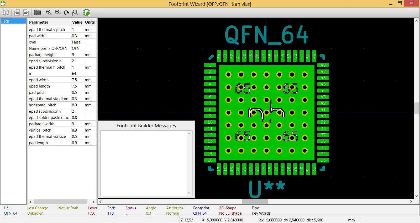
Open the footprint from the library or from the board. Make the required changes (pad size, courtyard expansion, silkscreen cleanup). Save the modified version into a local or company library rather than overwriting the original global library entry. This prevents accidental updates from breaking other projects.
Creating Reusable Libraries
Organize custom footprints into logical libraries (e.g., Company_Resistors, Company_Connectors, Project_Specific). Use consistent naming that includes the package and key dimensions. Document the source datasheet and revision date inside the footprint description field. Version-control the library folder so every engineer works with the same validated set.
A well-managed library reduces the risk that two boards in the same product family use slightly different land patterns for the same part number.
Footprint Verification Before Manufacturing
Before generating Gerbers, perform these checks:
- Run a full Design Rule Check with the manufacturer's minimum clearances loaded.
- Visually inspect every unique footprint in the 2D and 3D viewers.
- Confirm that pin 1 markers and polarity indicators are present and unambiguous.
- Export a centroid (pick-and-place) file and verify that the coordinates and rotations match the silkscreen.
- Cross-check the BOM manufacturer part numbers against the footprints actually used on the board.
Any footprint error that survives this stage will reach the fabricator and the assembler. Catching it now is far cheaper than discovering it after the first prototype run.
When the footprints are verified and the manufacturing files are ready, engineers can proceed to Gerber generation and order placement. Clean, consistent footprints are one of the strongest predictors of first-pass manufacturing success.
FAQ
Q1: What is the difference between a symbol and a footprint in KiCad?
A1: The symbol is the electrical representation used in the schematic (pins, pin types, power flags). The footprint is the physical land pattern used on the PCB (pads, silkscreen, courtyard). They are linked through the footprint assignment field but are stored in separate libraries.
Q2: How do I create a custom footprint in KiCad?
A2: Open the Footprint Editor, create a new footprint, place and size the pads according to the datasheet, draw the courtyard and silkscreen, assign a 3D model if needed, then save it into a local or company library. Always verify the pad numbers match the schematic pins.
Q3: Why does my KiCad footprint fail assembly even though DRC passed?
A3: Local DRC only checks the rules you configured. If the footprint pads, courtyard, or silkscreen do not match the real component or the manufacturer's process limits, assembly problems still occur. Always compare the footprint with the datasheet land pattern and the fabricator's design rules.
Q4: How should I organize custom footprints for multiple projects?
A4: Create dedicated company or project libraries, use consistent naming, document the source datasheet inside each footprint, and keep the libraries under version control. Avoid editing the global KiCad libraries directly.
Q5: Can I change a footprint after the PCB layout is finished?
A5: Yes. Use the "Change Footprints" tool or update the footprint assignment in the schematic and then update the PCB. After the change, re-run DRC and re-check clearances, because a different pad size or courtyard can introduce new violations.
```