Most PCB design work happens in 2D: pads, traces, and silkscreen. Yet every finished product must live in the physical world. Component height, connector orientation, and fit with the enclosure are all difficult to judge from a 2D view. KiCad's 3D visualization closes this gap. It is more than just a way to create attractive renders; it is an engineering tool that helps you:
-
Inspect the layout intuitively: See true physical sizes and relative positions of components.
-
Mitigate mechanical risk early: Catch tall capacitors that might hit the enclosure or connectors that could interfere with neighboring parts.
-
Improve manufacturability: Verify the orientation of connectors and switches for usability and assembly line efficiency.
-
Collaborate with mechanical engineers: Export a complete 3D board model (STEP) for direct use in MCAD workflows.
The sections below show how to obtain 3D models, associate them with footprints, fine-tune model alignment, use ray tracing for photorealistic renders, and automate exports via KiCad's CLI.
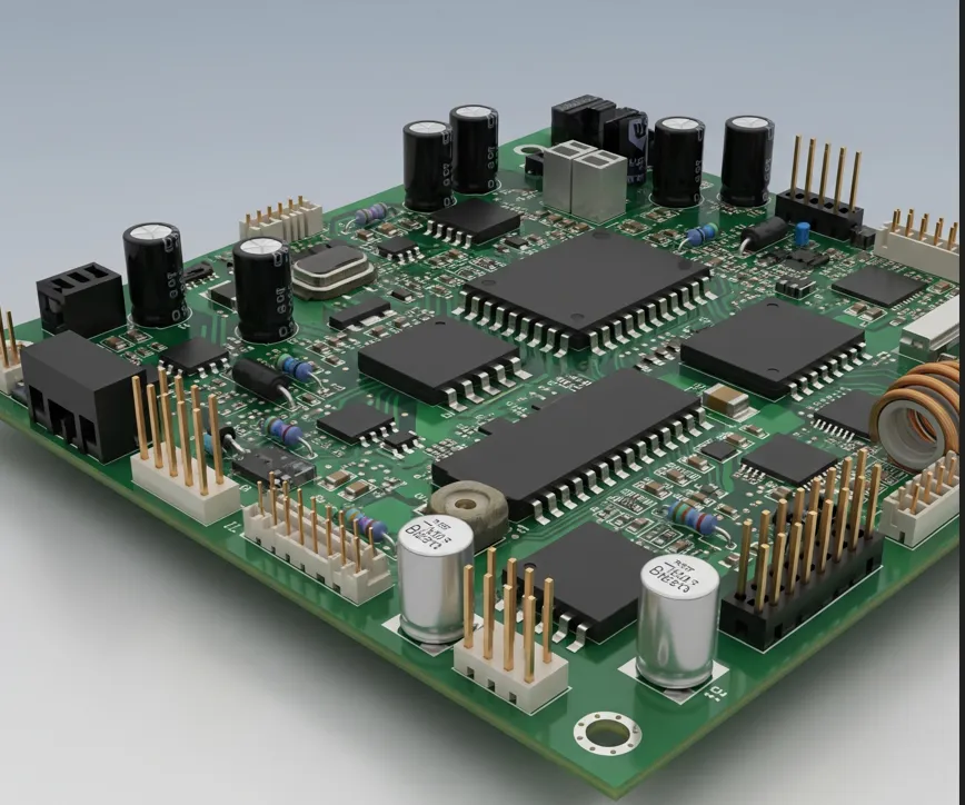
Where to Find 3D Models
Before linking models to footprints, you need suitable 3D files. Common sources include:
-
KiCad official library: The official 3D model library covers most standard packages and should be your first stop.
-
Component manufacturers: Major suppliers such as Molex, TE Connectivity, and Wurth Elektronik often provide accurate STEP models for connectors, inductors, and other key parts. These are generally the most reliable for MCAD.
-
ECAD content providers: Platforms such as SnapEDA, Ultra Librarian, and SamacSys frequently bundle 3D models alongside schematic symbols and PCB footprints.
-
General 3D repositories: Community libraries like the FreeCAD Electronics Library, GrabCAD, 3D ContentCentral, and TraceParts host a large variety of user-contributed models.
Tip: Prefer the .STEP format. STEP contains precise mechanical data and is the industry standard for ECAD–MCAD collaboration. The .WRL format is smaller and includes color information, making it useful for quick previews.
Linking a 3D Model to a Footprint
As an example, consider linking a downloaded 3D model to a USB Type-C receptacle footprint.
Step 1: Open Footprint Properties and Add the Model
-
In KiCad's PCB Editor or Footprint Editor, select the footprint you want to associate with a 3D model.
-
Press E to open the Footprint Properties dialog.
-
Switch to the 3D Models tab.
-
Click the Add 3D Model button and select your prepared file (for example, USB_C_Receptacle.step).
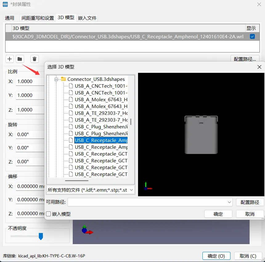
Step 2: Align the Model Precisely
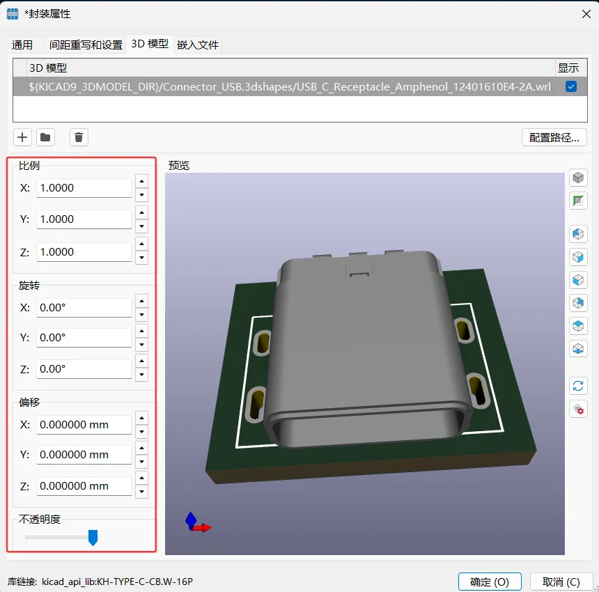
After adding the model, it may not align with the footprint in the preview. This is normal. Use the parameters below to align it accurately:
-
Scale: Adjust if the model's units differ from KiCad's. If a model was built in inches and your project is in millimeters, use scale to reconcile the difference. In most cases, keep X, Y, and Z at
1. -
Rotation: This is often the critical step. Rotate around the X, Y, and Z axes to align pins and pegs with SMD pads and through-holes.
-
Offset: Translate the model in X, Y, and Z to center it over the footprint. The Z offset is particularly useful to place the model's base exactly on the PCB surface.
Practical workflow: Don't try to nail it in one move. First correct Z-axis rotation to set the orientation. Then adjust X/Y offsets to center the model. Next, refine X/Y rotations for any tilt. Finally, tweak the Z offset to seat the model perfectly onto the board. The preview updates in real time, so alignment is highly visual.
Step 3: Preview the Full 3D Board
Click OK to save and return to the PCB Editor. Open the 3D Viewer with Alt+3 (or View → 3D Viewer). KiCad renders the entire board instantly. Use the left mouse button to rotate, the scroll wheel to zoom, and the middle button to pan. Your USB?C connector should now appear correctly "soldered" to the virtual PCB.
Embedding 3D Models into PCB or Footprint Libraries
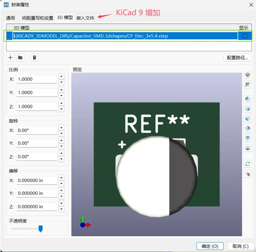
In versions prior to KiCad 9, STEP models and footprints were separate files referenced by path. Sharing a PCB required sending the 3D models as well; otherwise, models would not display.
KiCad 9 adds file embedding, allowing you to embed 3D models into the PCB or into the footprint itself. While embedding increases file size, it ensures complete 3D visualization when a PCB file is shared or archived—no separate 3D assets are needed.
Ray Tracing and Advanced Rendering
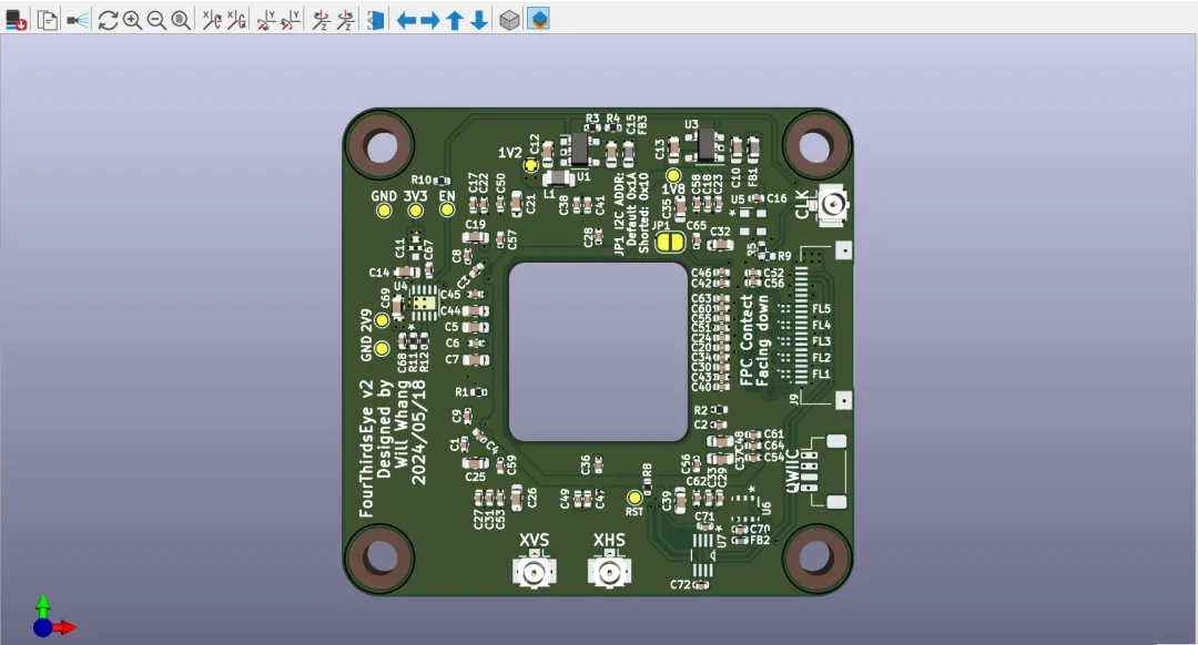
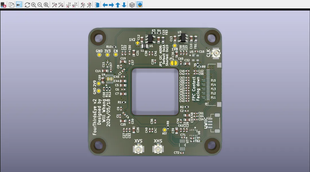
The 3D Viewer includes a powerful rendering engine with optional ray tracing. When enabled, it uses physically based rendering to simulate light transport in the scene—reflection, refraction, and realistic materials—producing near-photographic images of your PCB.
Open the 3D Viewer and go to Settings → Preferences → 3D Viewer to access advanced options and enable ray tracing.
Compare renders with and without ray tracing by toggling the setting and changing camera angles. The difference in shadows, reflections, and perceived material properties is substantial.
Automating 3D Exports with the CLI
From the PCB Editor, you can export various 3D formats manually via File → Export, including STEP, GLB, BREP, XAO, PLY, and STL.
However, repetitive exports or integration into automation (for example, CI/CD pipelines) is more efficient using KiCad's command-line interface, available in KiCad 7.0 and later. With a single command, you can generate a STEP model of the full assembly:
kicad-cli pcb export step [options] <input_file.kicad_pcb>
For example, to export MyProject.kicad_pcb to MyProject.step:
kicad-cli pcb export step --output "MyProject.step" "MyProject.kicad_pcb"
This produces a single STEP file containing all associated 3D models. It's ideal for batch processing multiple projects or generating deliverables on a build server.
Conclusion
Adding 3D models to your PCB design is a rigorous, efficient engineering practice. It gives you early visibility into mechanical realities, reduces rework risk, streamlines assembly considerations, and enables tight ECAD–MCAD collaboration. With accurate models, careful alignment, embedded assets for portability, photorealistic rendering via ray tracing, and CLI automation, KiCad provides a complete, production-ready 3D workflow for PCB and PCBA design.
Integrate these steps in your next KiCad project to validate form, fit, and function early and confidently.