










-
 19:28
19:28
KiCad 10 Features: What These Updates Change in PCB Design
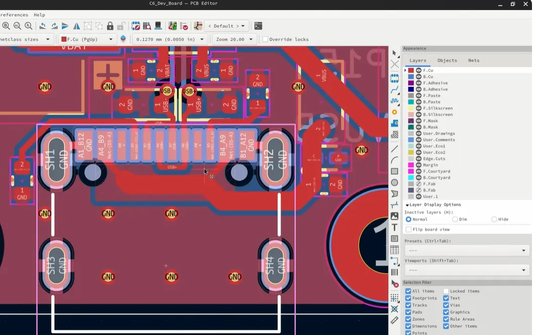
This video reviews KiCad 10 and FreeCAD 1.1, highlighting open-source updates that make schematic reuse, PCB layout, and enclosure design more efficient. For KiCad 10, it covers STEP-only official 3D models, directory-style symbol libraries, Windows dark mode, schematic variants for alternate BOMs and DNP components, hop-over wire display, schematic groups, and reusable PCB design blocks. Practical examples include a voltage-regulator block and USB-C connector routing that can be reused across PCB prototype projects. FreeCAD 1.1 improvements—including clearer selection, custom-origin transforms, quick measurement, projected external geometry, and internal-face generation—help engineers refine enclosures after the PCB outline is finalized. Together, these tools streamline the path from schematic and mechanical design to PCB assembly and online PCB quoting while reducing repetitive design work.
-
 31:48
31:48
Learn KiCad 10.0 in 7 Steps
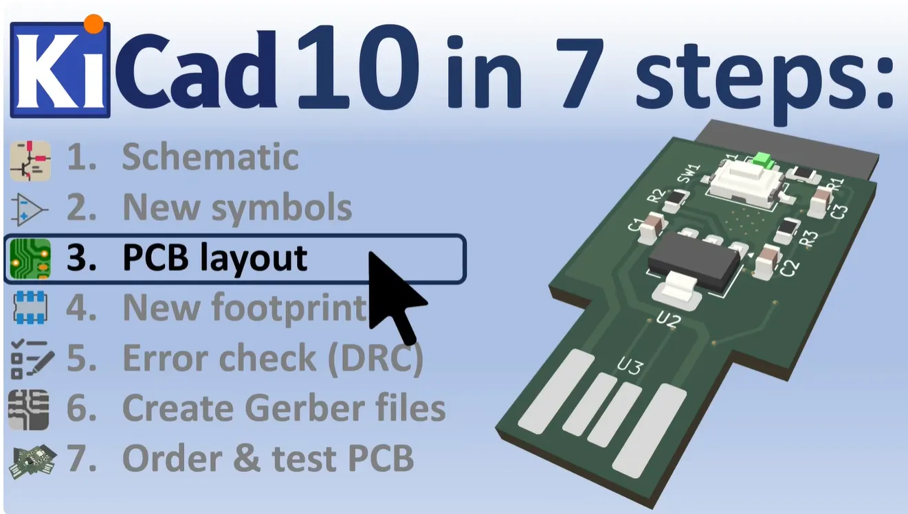
This video walks through a complete KiCad 10 PCB design workflow for an ESP32-S3 USB development board, covering project setup, schematic capture, custom USB connector symbol and footprint creation, wiring, global labels, board outline, component placement, silkscreen, routing, 3D review, and DRC. Using a compact two-layer FR4 PCB as an example, it highlights the manufacturing-critical details that determine first-pass success, including accurate pad geometry, copper-to-outline clearance, silkscreen clearance from pads, and a clean DRC. Once the design is verified, engineers can move directly from the completed files to an instant PCB quote or turnkey PCB assembly, making the workflow relevant to IoT, consumer electronics, PCB prototyping, and production-ready design handoff.
-
 01:38
01:38
AIVON KiCad Plugin: Order PCB From KiCad
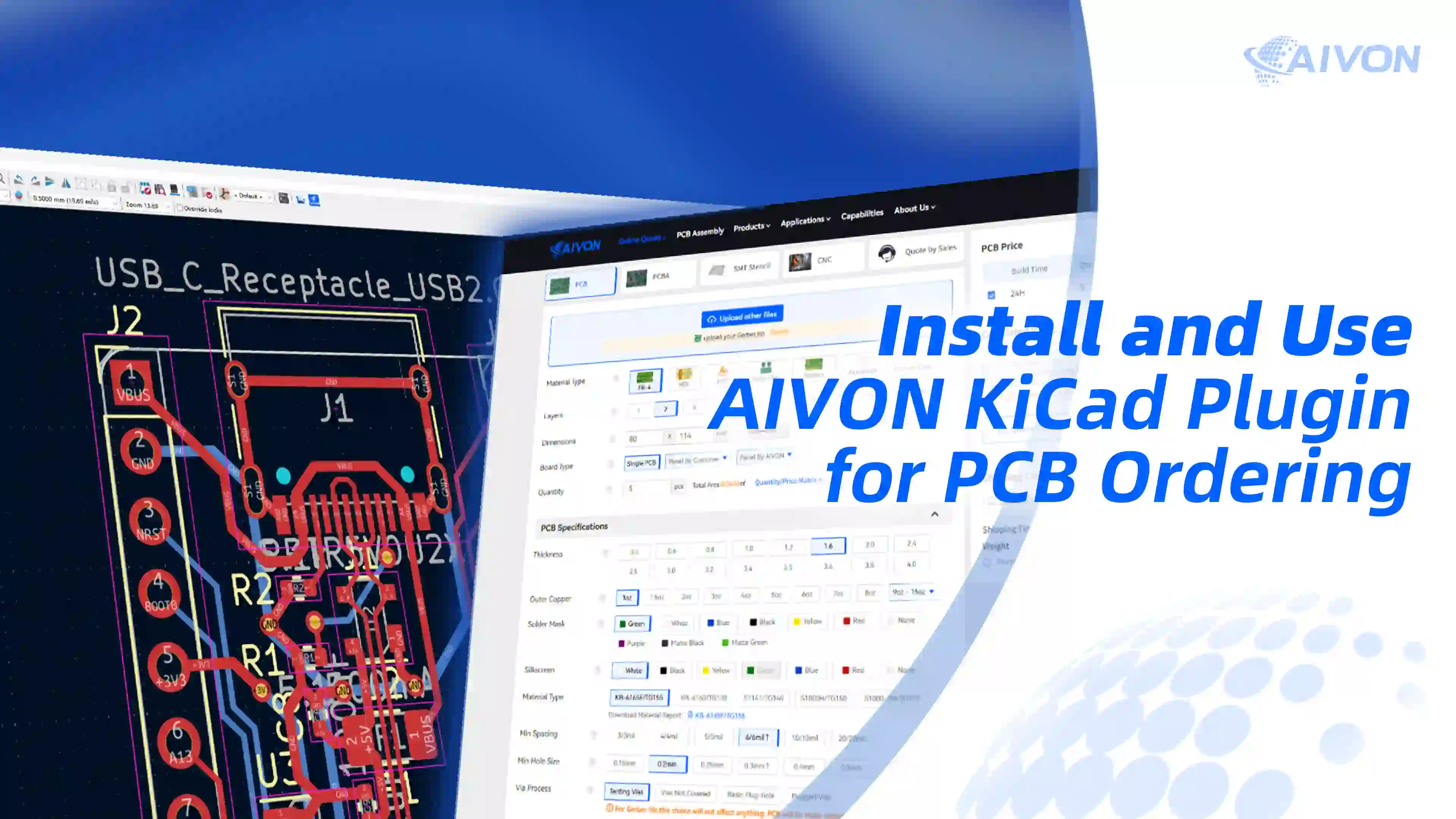
This tutorial demonstrates how to install the free AIVON KiCad plugin and streamline the workflow from a finished PCB layout to a production-ready order without manually exporting Gerbers or uploading files separately. It walks through KiCad’s Plugin and Content Manager, the Fabrication Plugins tab, applying pending changes, and launching the AIVON toolbar directly from the PCB Editor. Before quoting, the video emphasizes two critical checks—a clean DRC and a complete board outline—to ensure accurate CAM interpretation of board dimensions and layer count. Once launched, the plugin automatically extracts board parameters, packages manufacturing files, and opens a pre-filled instant PCB quote where engineers can confirm quantity, surface finish, solder mask color, and special requirements. The streamlined workflow supports both PCB prototype development and later PCB assembly quoting, helping IoT, industrial control, and consumer electronics teams reduce file-preparation errors and move from design freeze to fabrication more efficiently.
-
 00:27
00:27
From KiCad to PCB Order: AIVON Plugin Eliminates Manual Gerber Export
This video demonstrates how the AIVON KiCad plugin streamlines the journey from completed PCB design to an instant manufacturing quote directly within the CAD environment. Instead of exporting Gerber files, uploading them separately, configuring manufacturing options, and requesting pricing, engineers can use a simplified workflow to upload their design, review specifications, and receive a quote with fewer steps. The video highlights practical benefits such as faster PCB prototyping, reduced file-version errors, and smoother DFM communication. This workflow is especially useful for engineers developing rigid, multilayer, and mixed-technology PCBs for industrial, IoT, and consumer applications, helping shorten the path from design completion to PCB fabrication and assembly.


