Many hardware engineers and PCB designers face the same frustration: commercial EDA tools come with steep licensing costs, restrictive seat limits, and complex update cycles. For startups, open-source hardware teams, students, and independent makers, those barriers often delay prototypes or force compromises on design quality. KiCad solves this by delivering a complete, professional-grade PCB design suite that is free, open source, and capable of taking a design from schematic to manufacturing-ready files without artificial limits.
This article explains what KiCad is, the practical tasks you can complete with it, its core strengths, who benefits most from using it, and how the design workflow connects directly to real PCB fabrication and assembly. By the end, you will understand why KiCad has become a standard tool for producing reliable boards and how to move efficiently from layout to production.
What Is KiCad?
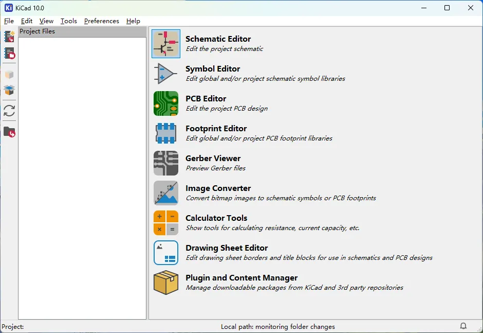
KiCad is a free, open-source electronic design automation (EDA) suite focused on printed circuit board design. It provides integrated tools for schematic capture, PCB layout, footprint and symbol library management, 3D visualization, electrical and design rule checking, and generation of manufacturing outputs such as Gerber files, drill files, BOMs, and pick-and-place data.
Unlike fragmented toolchains that require exporting netlists between separate programs, KiCad keeps schematic and board data synchronized inside a single project. The current stable release (KiCad 10.x series) runs on Windows, macOS, and Linux and supports everything from simple two-layer prototypes to multi-layer boards with controlled impedance, differential pairs, and complex hierarchical designs.
Engineers need KiCad when they require full design ownership without recurring license fees, when they want transparent, community-reviewed libraries, or when they must generate clean fabrication files that fabricators can process without conversion issues.
Why KiCad Is Becoming Popular Among PCB Designers
Commercial tools still dominate large corporations with dedicated CAD teams, but KiCad adoption has grown rapidly among the broader engineering community for practical reasons:
- Zero cost of entry and no seat restrictions mean entire teams or classrooms can use the same version.
- The interactive push-and-shove router and modern selection tools reduce the time spent fighting the software during dense layouts.
- High-quality official libraries plus community-maintained repositories cover most common parts, reducing the need to create every footprint from scratch.
- Regular major releases (now on a yearly cycle with continuous point releases) add features requested by practicing designers—zone management, improved net inspection, better STEP export, and enhanced DRC rules—without forcing users onto paid upgrade paths.
- Because the source is open, companies can audit the software, contribute fixes, or embed it into internal workflows.
From a manufacturing perspective, the popularity also stems from reliable output generation. Fabricators receive consistent Gerber, Excellon, and ODB++ files that pass automated DFM checks more reliably when designers follow KiCad's design-rule and net-class settings.
What Can You Do with KiCad?
KiCad covers the complete design-to-manufacturing chain. Below is how each major capability fits into real engineering work.
Schematic Design
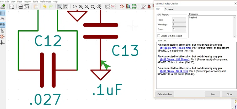
The Schematic Editor supports single-sheet and multi-level hierarchical designs. You place symbols from the official or custom libraries, assign footprints, define net classes, and run the Electrical Rules Checker (ERC) to catch floating pins, power conflicts, and connectivity errors before layout begins.
Best practice: Assign net classes early (power, high-speed, sensitive analog) so the same constraints automatically transfer to the PCB editor. A common mistake is treating the schematic as a drawing only; engineers who skip ERC often discover missing connections only after copper has been poured.
Manufacturing link: Clean schematic data produces accurate BOMs and component position files later. Incomplete or duplicated reference designators create assembly errors that increase cost and delay.
PCB Layout
The PCB Editor provides interactive routing, differential-pair tools, zone fills, and multi-channel layout support. Design Rule Check (DRC) runs continuously or on demand against clearance, track width, via size, and custom rules you define.
Recommended workflow:
- Import the schematic (netlist is handled internally).
- Set board outline and stack-up.
- Place critical components first (connectors, high-speed ICs, power stages).
- Route with push-and-shove enabled.
- Run DRC and correct violations before generating outputs.
Common layout mistakes that cause manufacturing problems include insufficient annular ring, acute angles that create acid traps, and copper-to-edge clearances that violate fabricator minimums. Professional engineers always load the target fabricator's design rules into KiCad's constraint system before final routing.
Footprint Management
KiCad's Footprint Editor and library system let you create, edit, and associate footprints with symbols. Official libraries follow IPC standards for land patterns; community libraries fill gaps for less common parts. You can also import footprints from other formats when needed.
Engineering tip: Always verify pad sizes, silkscreen clearance, and courtyard against the component datasheet and the fabricator's capabilities. Undersized pads or missing solder-mask openings are frequent causes of assembly defects.
3D Visualization
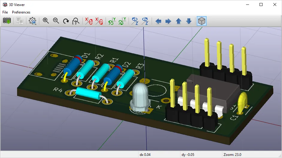
The integrated 3D Viewer renders the board with component models (STEP or VRML). Ray-traced views help check mechanical fit, component height conflicts, and overall aesthetics before ordering.
Use the 3D view after placement and again after routing. Catching a tall capacitor colliding with a connector or a mounting hole blocked by copper saves a revision cycle. Export options allow selective STEP output for mechanical CAD collaboration.
Manufacturing Output
KiCad generates the complete set of files required by fabricators and assemblers:
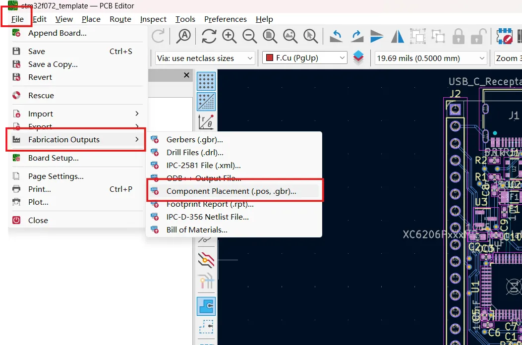
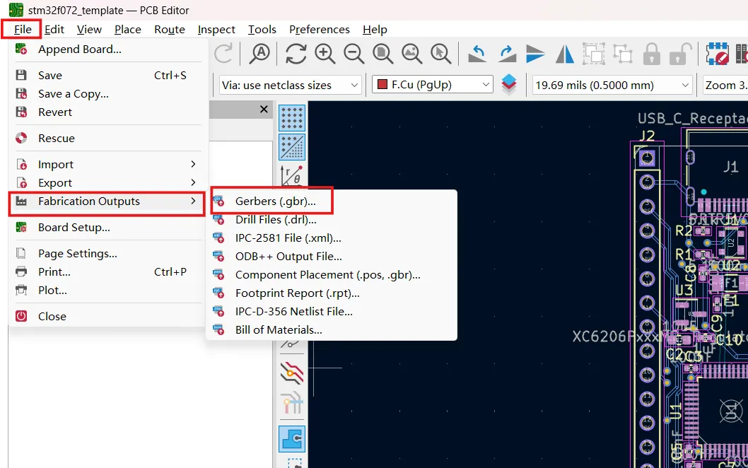
- Gerber (or Gerber X2) layers
- Excellon drill files
- Pick-and-place (centroid) files
- BOM
- Optional ODB++ and PDF fabrication drawings
The Plot and Drill dialogs let you control layer mapping, mirror options, and aperture settings. After export, open the files in GerbView (included with KiCad) to verify that copper, solder mask, and silkscreen align correctly.
DFM consideration: Always run a final DRC with the fabricator's minimum track/space and annular-ring values loaded. Many boards fail first-article inspection because designers used default KiCad rules instead of the actual process capabilities of the chosen manufacturer.
Key Features of KiCad
Open Source
The entire codebase is available under an open-source license. This transparency allows security audits, custom plugins via the IPC API, and long-term independence from any single vendor's business decisions.
Free to Use
There are no feature tiers, no board-size limits, and no mandatory cloud accounts. The same software used for a student project can produce production boards for a commercial product.
Cross-Platform Support
Native builds exist for Windows, macOS, and Linux. Project files are portable across operating systems, which is valuable for distributed teams and for engineers who switch machines.
Active Community
Thousands of users contribute libraries, plugins, documentation, and bug reports. Forums, Discord channels, and annual events such as KiCon provide rapid answers and shared design practices. The community-driven libraries reduce the time spent recreating common footprints.
Who Should Use KiCad?
- Beginners and engineering students – The learning curve is manageable, and the free nature removes cost barriers. Students can produce real Gerber files and order boards without institutional software licenses.
- Hardware engineers and small product teams – Full schematic-to-fabrication capability supports professional work while avoiding annual license renewals.
- Makers and open-source hardware creators – Designs can be published with complete KiCad source so others can modify and reproduce the boards.
- Open-source developers – The transparent toolchain aligns with open-hardware principles and simplifies collaboration.
In each case the same core workflow applies: design → ERC/DRC → manufacturing file generation → DFM review → fabrication and assembly.
How AIVON Supports KiCad Users
After the KiCad design process is complete—DRC clean and the board ready for production—engineers still need a fast, reliable path to physical boards. AIVON connects directly with KiCad through a dedicated plugin that simplifies this final step.
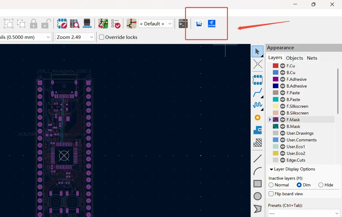
With the AIVON plugin installed, users can click a single button inside the KiCad PCB Editor. The plugin transfers the current design data and opens the AIVON ordering page, so there is no need to manually export Gerber files, drill files, or assembly data and upload them separately. This removes a common source of file mismatches and saves time between finishing the layout and placing an order.
AIVON then performs automated DFM checks against standard process limits and returns a quotation for bare boards or fully assembled PCBs. The designer retains full control of the original KiCad source files while the manufacturing hand-off becomes a one-click action instead of a multi-step file-preparation task.
This direct plugin workflow shortens the gap between a verified layout and functional hardware, letting engineers move from design to production with fewer manual steps and lower risk of transfer errors.
FAQ
Q1: Is KiCad good enough for professional PCB design?
A1: Yes. Many engineers and small companies use KiCad for production boards. The combination of interactive routing, customizable design rules, 3D verification, and reliable Gerber export meets the needs of most commercial projects that do not require the most specialized high-speed or RF tool suites.
Q2: What is the latest version of KiCad and where can I download it?
A2: As of mid-2026 the stable release is in the 10.0.x series. Official downloads for Windows, macOS, and Linux are available at kicad.org/download. Always use the stable release for production work.
Q3: Can I generate manufacturing files directly from KiCad for any PCB fabricator?
A3: Yes. KiCad produces industry-standard Gerber, Excellon, BOM, and centroid files. Most fabricators accept these files. Load the specific design rules of your chosen manufacturer into KiCad's constraint system before the final DRC to minimize DFM issues.
Q4: Does KiCad support multi-layer boards and controlled impedance?
A4: Yes. You can define stack-ups, assign net classes with specific trace widths and clearances, and route differential pairs. For controlled-impedance designs, calculate the required geometry with a stack-up calculator and enter those values as design rules.
Q5: How does KiCad compare to paid tools for beginners who later need professional results?
A5: Beginners can start without cost and later apply the same projects and libraries in professional environments. The learning investment transfers directly, and the manufacturing file quality is equivalent to that of many commercial tools when design rules are properly configured.