










7,500 m²
Class 10K Cleanroom
From component sourcing and SMT assembly to testing and final inspection,
discover how AIVON turns your PCB designs into reliable assembled boards.

Class 10K Cleanroom
Production Lines
SMT Mounting Points/Day
From SMT placement and THT soldering to assembly and testing, our PCBA facilities are equipped to support every stage of the manufacturing process. With 7 Siemens SMT lines, 3 DIP lines, and 3 assembly & testing lines, we deliver consistent production across different order volumes.
Our facilities can handle up to 10 million SMT mounting points and 180,000 THT soldering points per day, providing the capacity to move efficiently from production to final testing.
The PCBA manufacturing process begins with preparing the bare PCB, components, and production data. The engineering team reviews the PCB design, BOM, and component information to make sure the materials and assembly data are ready for production. Components are also checked against the BOM before they are released to the SMT line.
At this stage, the PCB and components need to be properly stored and handled to prevent issues such as moisture, contamination, or component mix-ups during assembly.
Once the PCB and production materials are ready, solder paste is applied to the appropriate pads on the PCB using a stencil printer. The stencil defines where the solder paste is deposited, while the squeegee controls how the paste is transferred onto the board.
The amount and position of solder paste are important because they directly affect the quality of the solder joints during reflow. Printing parameters such as stencil alignment, squeegee pressure, and printing speed need to be properly controlled for consistent results.
After solder paste printing, the PCB passes through a Solder Paste Inspection (SPI) machine to check whether the paste has been applied correctly. SPI equipment uses 3D imaging to measure factors such as solder paste volume, height, area, and position.
This inspection helps identify problems such as insufficient solder paste, excessive paste, or paste offset before components are placed. Detecting these issues at this stage allows them to be corrected before they become soldering defects later in the process.
After the solder paste has been inspected, the PCB moves to the pick-and-place machine. The machine automatically picks components from feeders and places them onto the corresponding PCB pads according to the assembly data.
Placement accuracy is particularly important for small and fine-pitch components, where even a small deviation can affect soldering quality. The placement program, component orientation, feeder setup, and machine calibration all need to be properly controlled before production.
With the components placed on the PCB, the board enters the reflow oven to permanently solder the components in place. The PCB passes through several controlled temperature zones, typically including preheating, soaking, reflow, and cooling.
During the reflow stage, the solder paste melts and forms solder joints between the component terminals and PCB pads. A suitable temperature profile is important to achieve reliable solder joints while avoiding excessive thermal stress on the PCB and components.
After reflow soldering, the assembled PCB is inspected using Automated Optical Inspection (AOI). The AOI system uses cameras and image processing to compare the assembled board against the expected assembly data.
Depending on the equipment and inspection requirements, AOI can identify issues such as missing or misplaced components, incorrect component orientation, solder bridging, and other visible assembly defects. Boards with detected abnormalities can then be reviewed and corrected before moving to the next stage.
After the main assembly process is completed, the PCBA undergoes final inspection to verify its overall assembly quality. Engineers or quality inspectors check the board for visible defects and confirm that the required components have been correctly assembled.
Where functional testing is required, the assembled PCB is also tested under defined operating conditions to verify that it performs as intended. The specific test method depends on the product design and customer requirements.
Once the PCBA has passed the required inspections and tests, it is prepared for shipment. The finished boards are handled and packaged according to their requirements to help prevent damage, contamination, electrostatic discharge, and other issues during transportation.
At AIVON, PCBAs can be shipped using major international express carriers such as DHL, FedEx, and UPS, along with other shipping options based on the customer's requirements. The completed orders are properly labeled, packed, and prepared for delivery to help ensure a smooth and reliable shipping process.
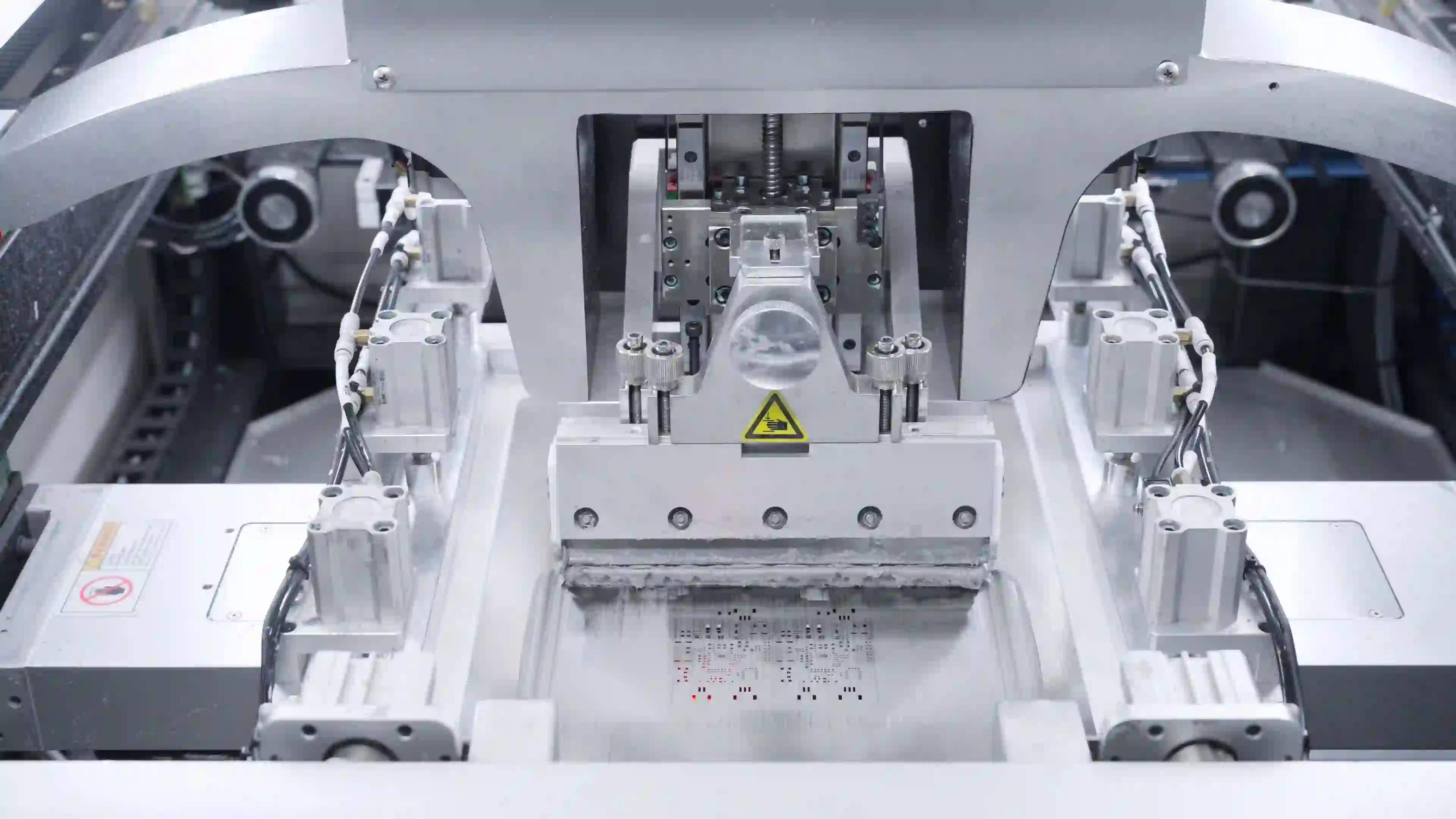
GKG-G5 Automatic Stencil Printer
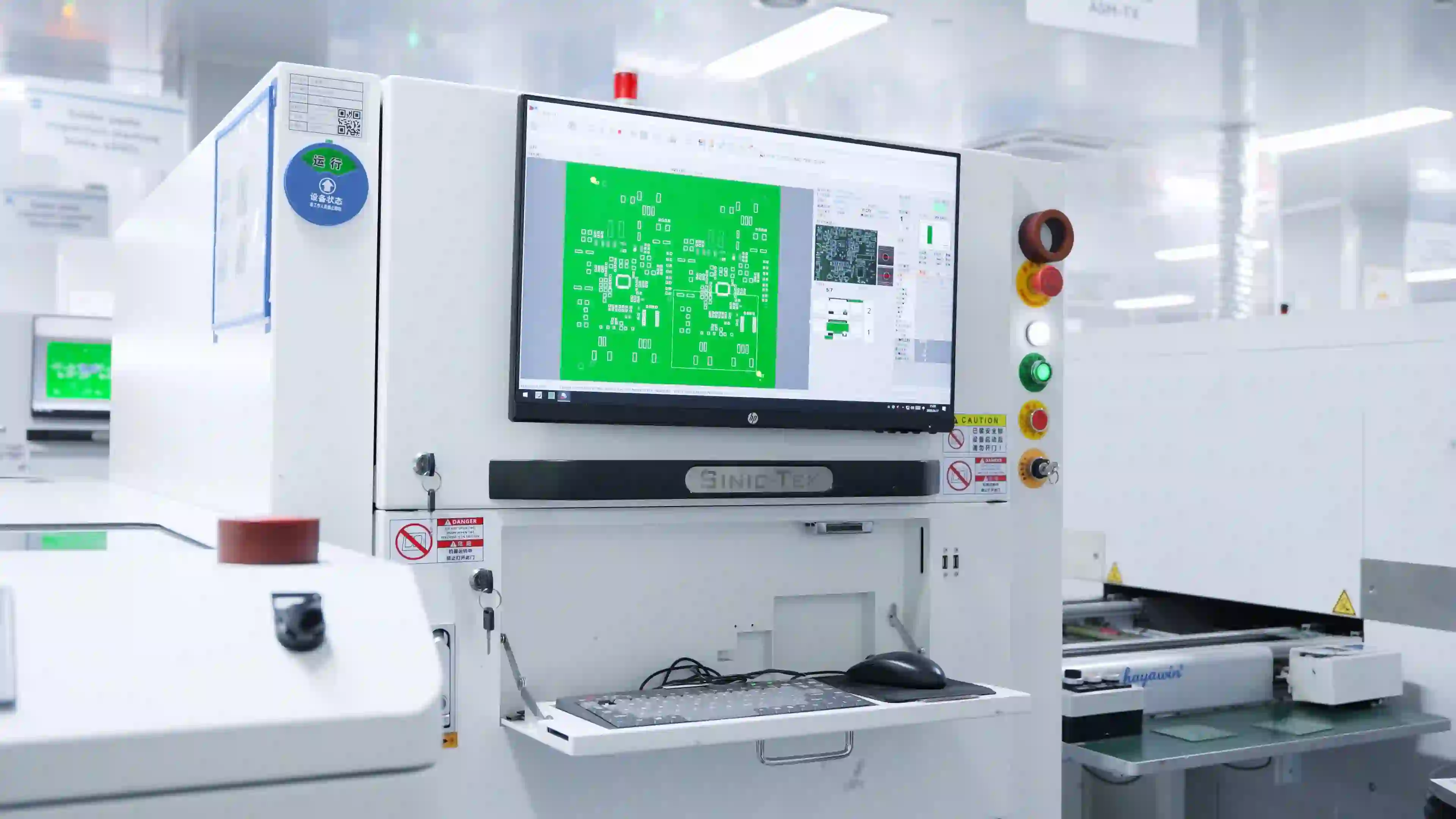
JT Solder Paste Inspection System
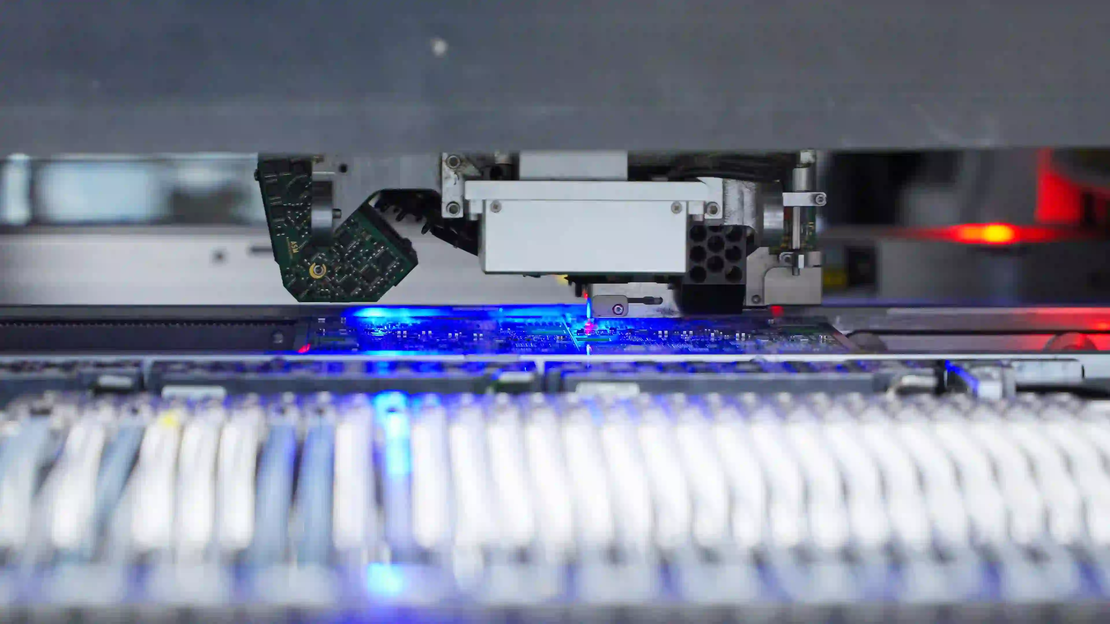
ASM Siemens High-Speed Pick-and-Place Machine
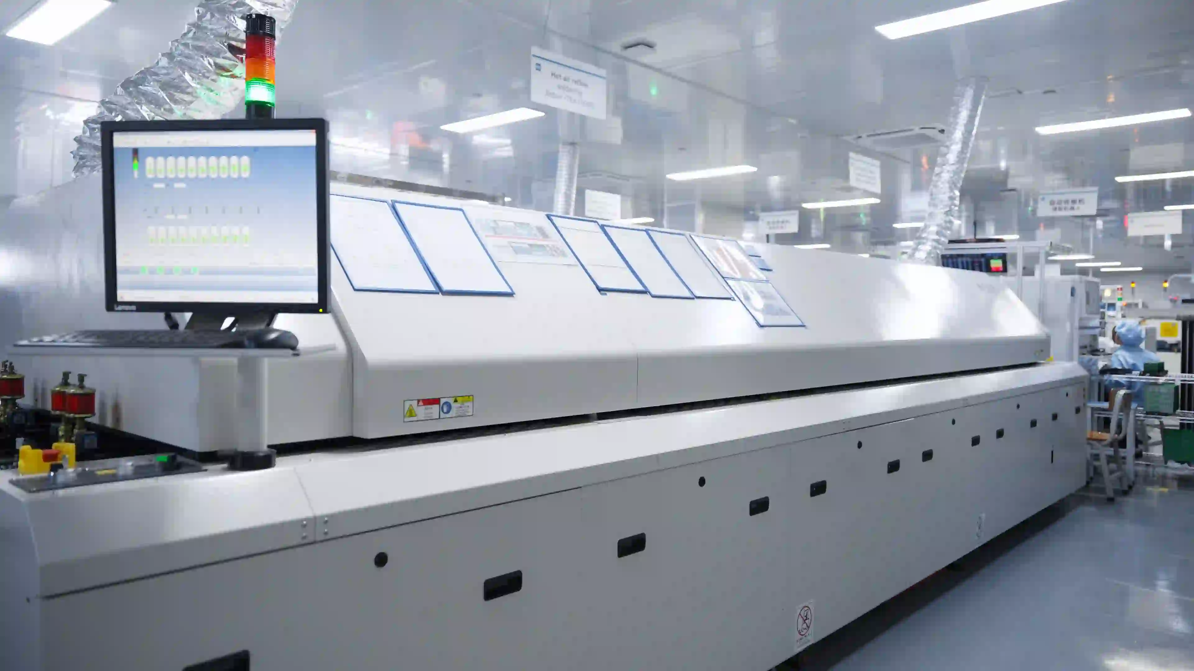
JT Reflow Oven
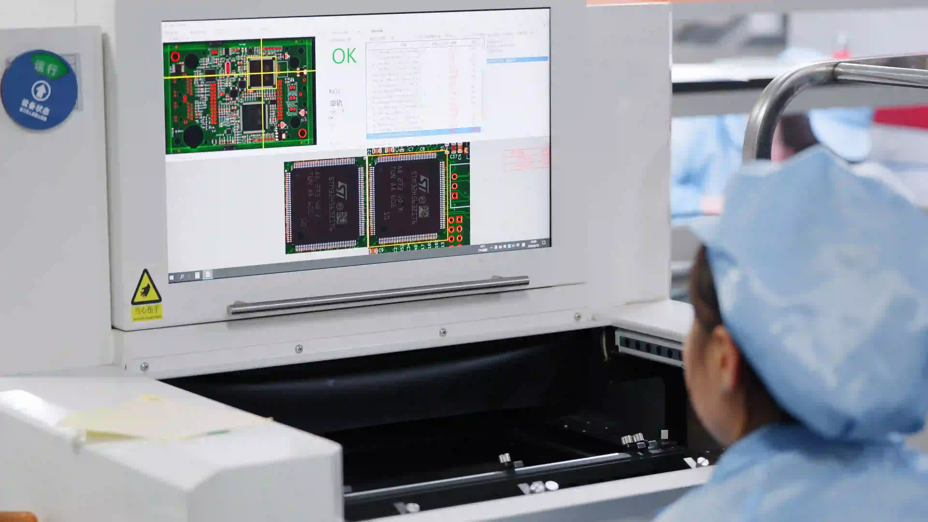
EAGLE 3D In-Line AOI Inspection System
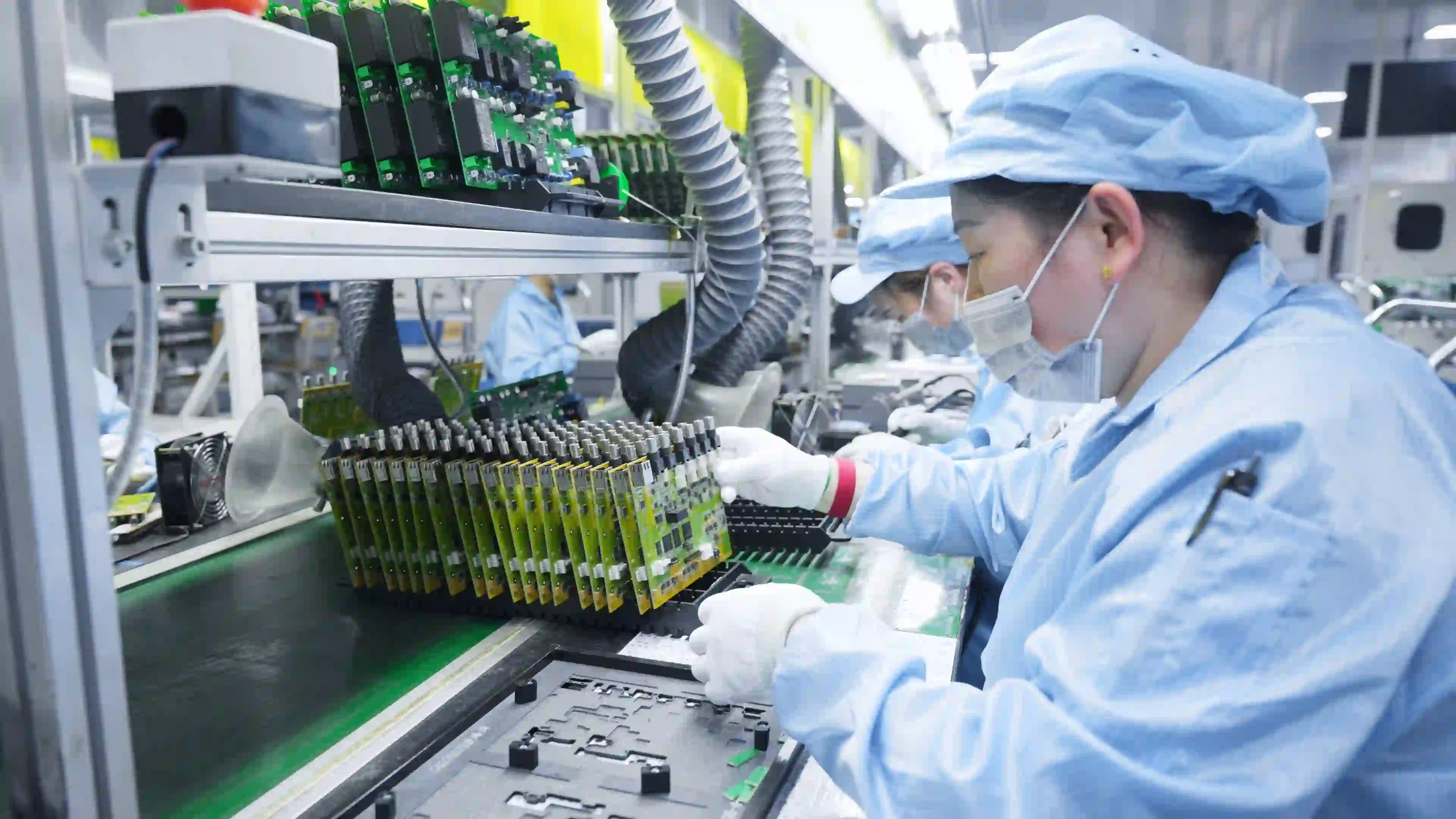
Through-Hole Component Assembly
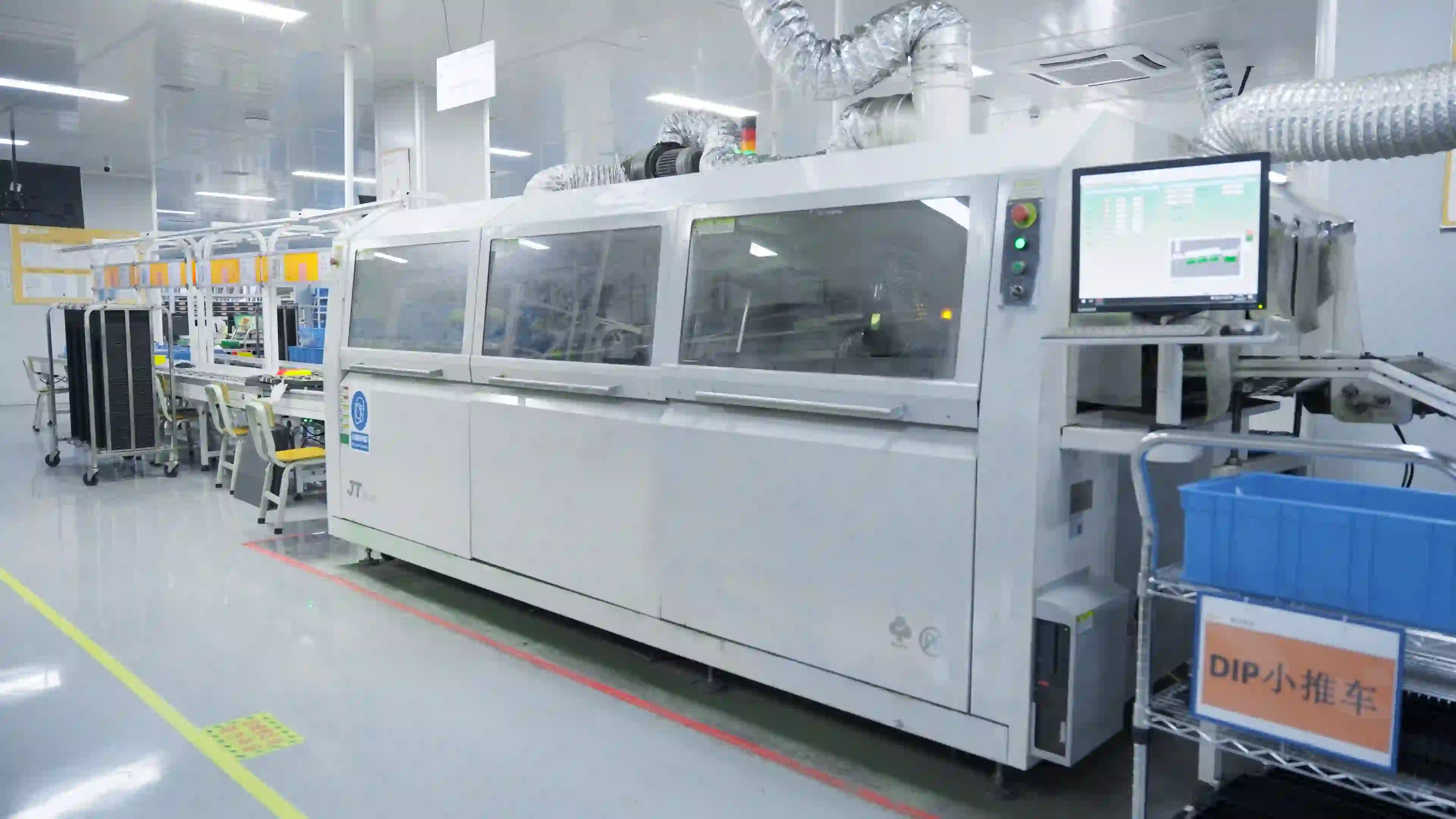
JT-SE350 Wave Soldering Machine
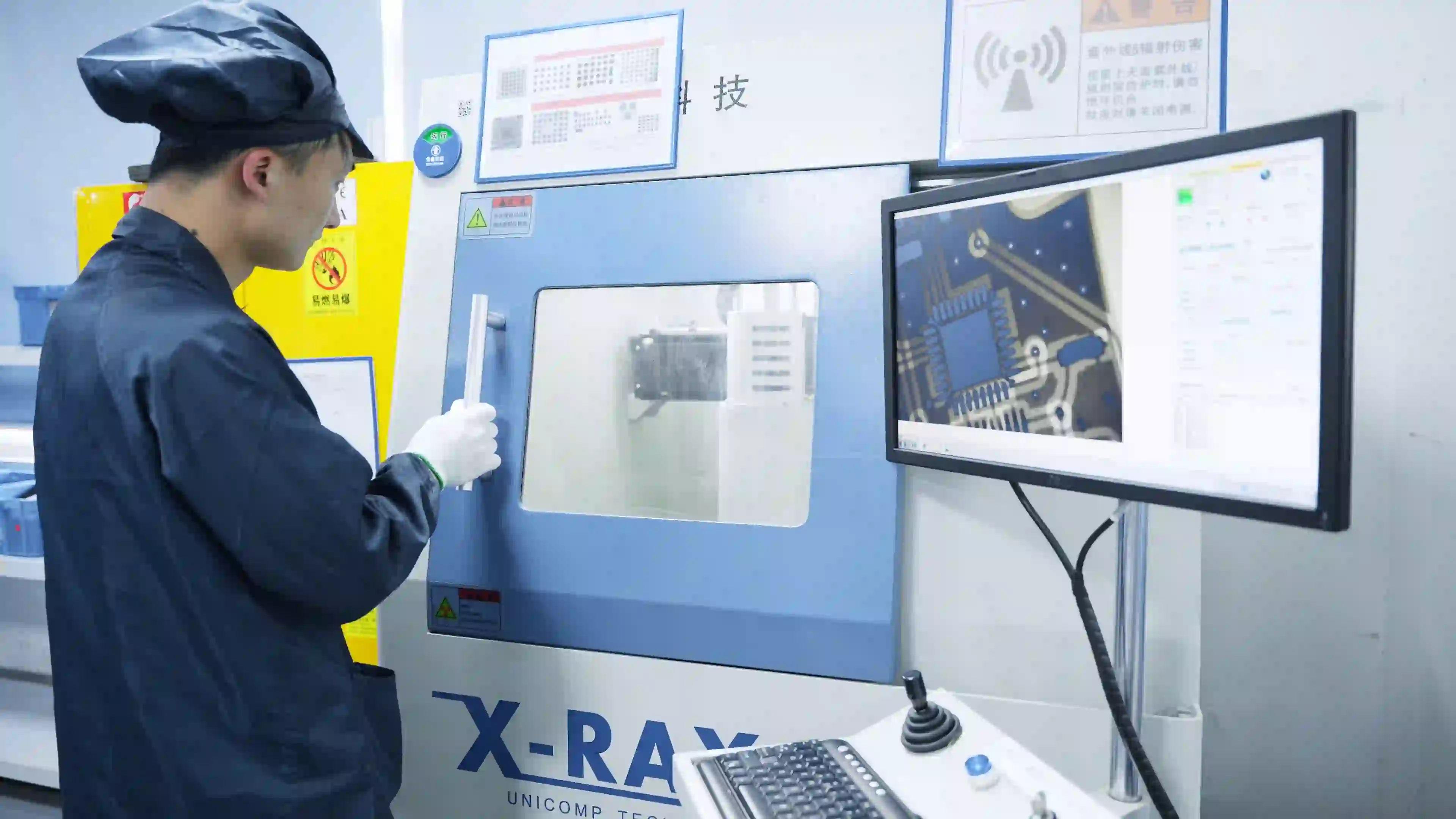
Unicomp X-Ray Inspection System
| Category | Capability |
|---|---|
| Type | SMT and THT |
| MOQ | No MOQ required for customers with R&D purposes |
| Component Size | 01005 chip size |
| Component Package | We accept tape and reel, tube, and tray packages for components |
| Maximum Mount Accuracy of Components (100FP) | ±50μm |
| Solderable PCB Type | Rigid PCB, FPC, Rigid-Flex PCB, Aluminum PCB |
| Size | Min: 50mm x 50mm, Max: 1200mm x 350mm |
| Board Thickness | 0.5mm-5mm |
Real PCBA Case Studies
Our engineering team reviews your PCB data, BOM, and assembly requirements before production to identify potential manufacturing issues early.
Each PCBA goes through a structured manufacturing process, with inspection and process controls at key stages from solder paste printing to final testing.
SPI and AOI inspections help detect solder paste and assembly defects during production, allowing issues to be identified and corrected before final delivery.
A1: SMT places components directly onto the surface of the PCB, while THT inserts component leads through holes in the board before soldering. SMT is commonly used for compact, high-density assemblies, while THT is often used for components that require stronger mechanical connections. Many PCBAs use a combination of SMT and THT assembly.
A2: The lead time for PCBA production depends on factors such as order complexity, component availability, production quantity, and testing requirements.
For prototype and small-volume orders, AIVON can provide a fast production schedule once the PCB files, BOM, and required components are confirmed.
For a more accurate lead time based on your project requirements, please contact our team for a quote and production schedule.
A3: Yes. AIVON can source components for PCBA assembly based on your BOM, helping simplify procurement and coordinate components with the PCB assembly process. Our team can also review component availability and potential alternatives when required.
Get in touch with our Turnkey PCB Assembly specialists for a quote today.
Send Inquiry


