-
 00:39
00:39
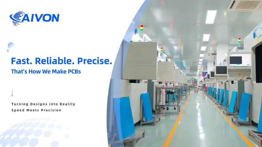
Fast. Reliable. Precise. That’s How We Make PCBs
Take a behind-the-scenes look at AIVON’s advanced PCB manufacturing facility and discover how automation, precision engineering, and strict quality control work together to produce high-performance printed circuit boards. This video showcases high-speed CNC drilling, automated solder mask processing, and cleanroom manufacturing environments designed to ensure dimensional accuracy, excellent signal integrity, and reliable thermal performance. From FR4 and high-frequency PCBs to rigid-flex designs, AIVON’s streamlined production process supports both rapid prototyping and high-volume manufacturing, delivering consistent quality for demanding applications in the medical, automotive, aerospace, and industrial sectors.
-
 00:31
00:31
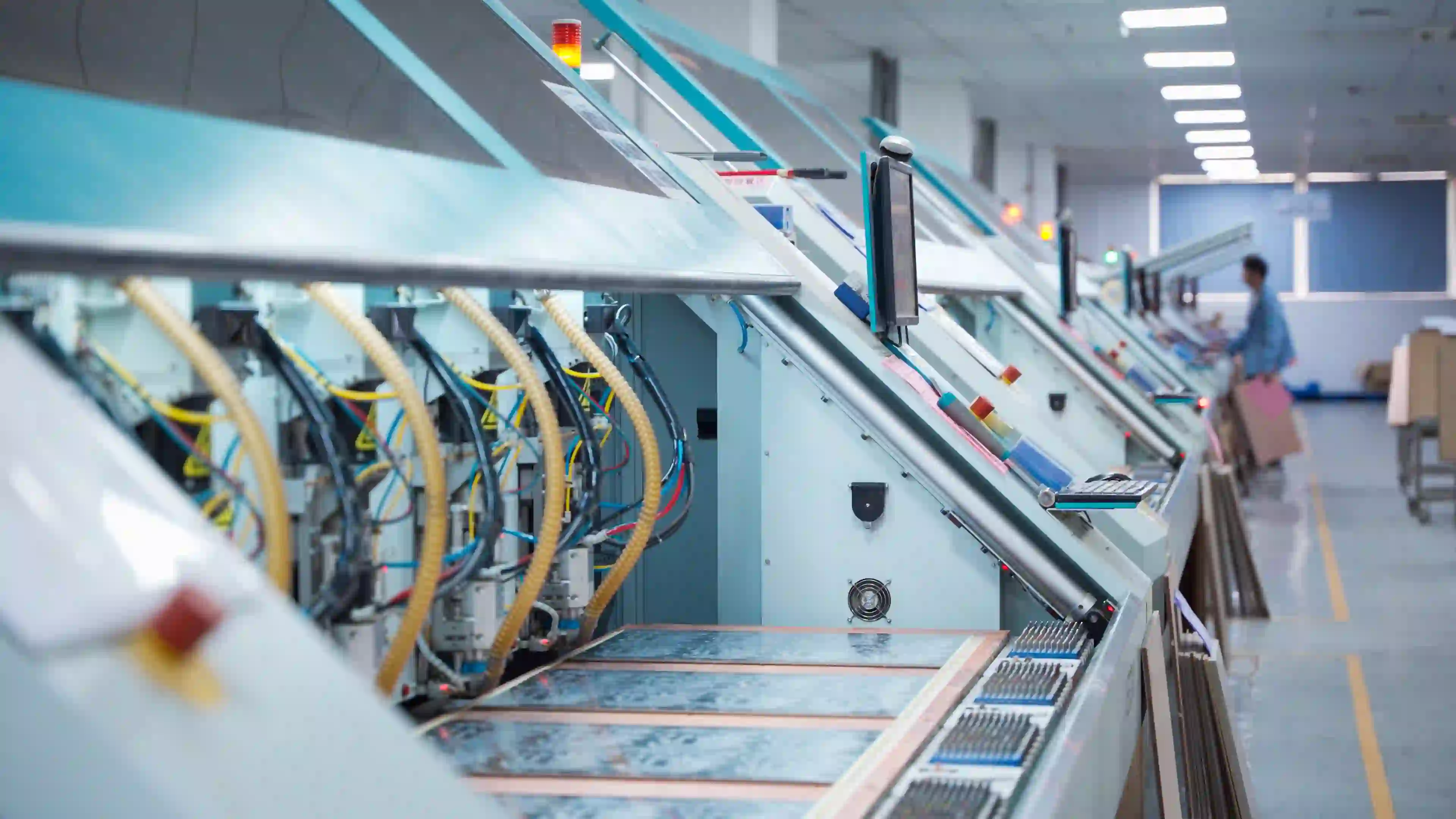
The PCB Manufacturing Process in Action
Experience the pulse of modern innovation in this dynamic behind-the-scenes tour of the AIVON facility. Witness a seamless transformation as raw materials evolve into complex, high-performance circuitry through our fully integrated and synchronized production lines. From the rapid-fire precision of automated drilling to sophisticated plating chemistry and high-speed optical systems, discover how we maintain peak consistency in a pristine, climate-controlled environment. See how we turn complex engineering designs into reality with unmatched industrial scale and surgical accuracy. This is the art of assembly—redefined.
-
 00:40
00:40
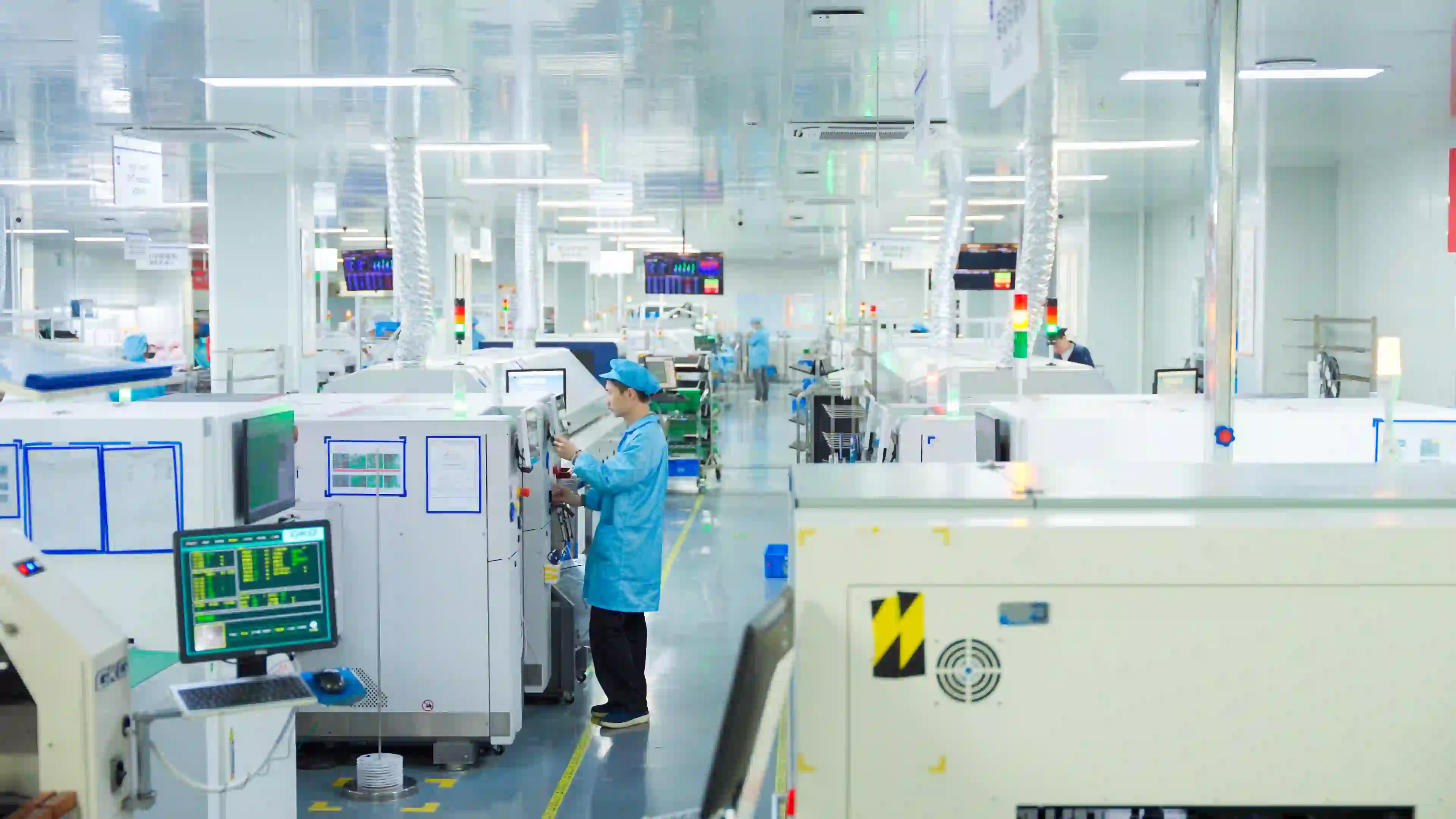
How We Build Your PCB at AIVON
How does a digital design transform into the high-performance heart of a modern device? Step inside the AIVON facility to witness the perfect synergy of advanced automation and expert human oversight. From the surgical accuracy of high-precision LDI imaging and ultra-fast CNC drilling to our rigorous zero-defect testing, we reveal the uncompromising quality built into every layer. Discover how our pristine, controlled environment and meticulous process control empower mission-critical projects in the aerospace, medical, and automotive sectors. At AIVON, we don’t just manufacture boards—we engineer reliability.
-
 00:31
00:31
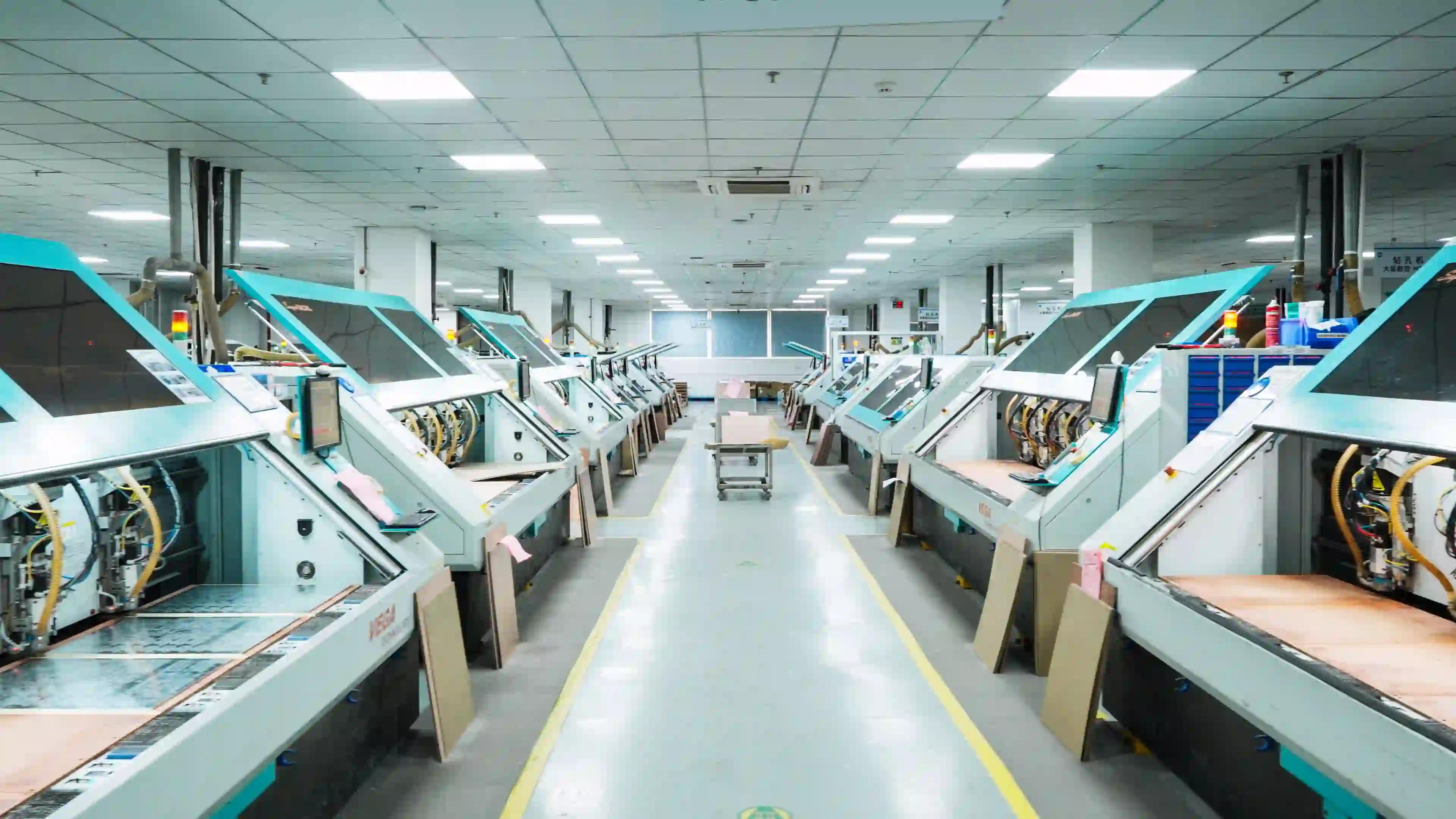
Inside AIVON PCB Factory: Precision Manufacturing Process
Ever wondered how a raw substrate transforms into a high-performance circuit board? Step inside AIVON’s state-of-the-art facility for an exclusive look at the heart of modern electronics. From the clinical precision of our ultra-clean rooms to the blistering speed of our automated production lines, witness the journey of a PCB from etching and drilling to final inspection. Discover how we harmonize cutting-edge technology with rigorous quality control to deliver the reliability required by aerospace and medical sectors. This is where precision meets speed—this is the future of PCB fabrication.
-
 02:26
02:26
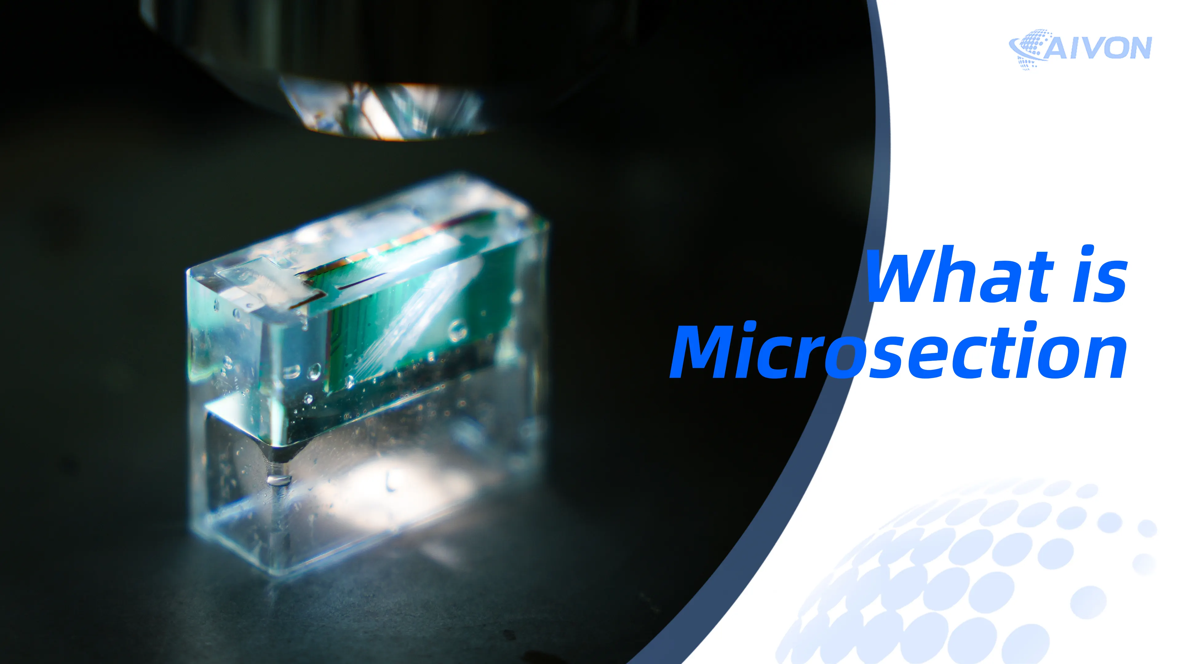
PCB Microsection Analysis: Cutting Open Boards to Find Hidden Failures
A PCB can look flawless on the outside while hiding "ticking time bombs" within its layers. How do you ensure your board won't fail under thermal stress or vibration? Welcome to the world of microsection analysis—the ultimate "truth test" for high-reliability electronics. By slicing through the board’s internal architecture, we reveal what standard tests miss: plating voids, thin copper, and layer misalignment. In this factory deep-dive, learn how this essential destructive test safeguards projects in the aerospace, medical, and automotive sectors. Don't just hope your PCB is reliable—verify it under the microscope.
- Products & Service
- Company
- About AIVON
- Contact
- News
- Blog
- Certification
-


- Payment
-


2026 AIVON.COM All Rights Reserved