Rigid-flex PCBs always demand extra attention during CAM review due to the complexity of combining rigid and flexible sections in one board. This case study examines order, a hybrid 8-layer rigid with 4-layer flex design. During our DFM engineering review, multiple critical issues required clarification, particularly around stackup definition, flex-rigid transition zones, and via-in-pad requirements under BGA areas.
Our CAM team identified several manufacturability concerns that could impact reliability and yield. Below is a detailed look at the engineering questions raised and how we resolved them to ensure successful production.
Order Overview
This was a rigid-flex PCB ( #RFP-20260324-002 ) with an 8-layer rigid section (FR-4 TG155, 1.0 mm thickness) and 4-layer flex area using Shengyi material. The design specified 1 oz copper on both inner and outer layers, ENIG surface finish with 1.0 µ" gold, 0.15 mm minimum hole size, and 4 mil trace/space. The order was for 5 pieces (5 sets). Special customer requirements included via-in-pad filling and capping on both sides for all vias under BGA chips. Production involved no panelization (1x1) with routing plus laser forming.
The combination of rigid-flex construction, high-density BGA via-in-pad requirements, and precise flex-rigid transition made this board particularly sensitive to DFM adjustments.
Main Engineering Questions Found During CAM Review
1. Rigid-Flex Stackup and Copper Weight Clarification
We noticed repeated discrepancies between the ordered copper weights (1 oz inner and outer) and the provided structure drawing. Our engineer reviewed the lamination details multiple times and recommended producing inner layers at 0.5 oz and outer layers at 1 oz to balance manufacturability, bend reliability, and electrical performance.
After several rounds of confirmation, including updated production stackup drawings, the customer approved our optimized structure. We suggested this adjustment because strict 1 oz on all layers could negatively affect flex region bendability and increase material stress.
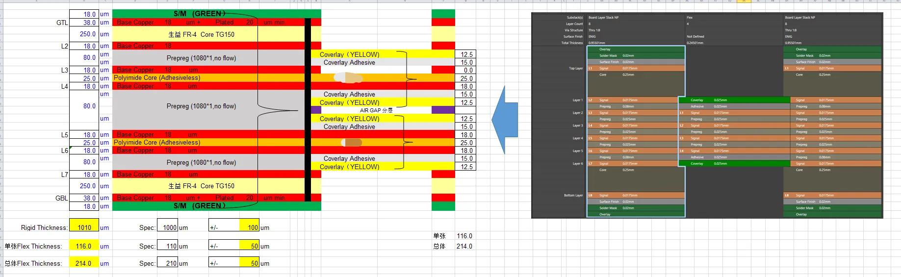
Figure 1: production stackup drawings
If ignored, using full 1 oz copper throughout could lead to stiffer flex sections, higher risk of delamination at the rigid-flex junction during repeated bending, or excessive board thickness variation beyond the specified 1.0 ±0.1 mm for the rigid part.
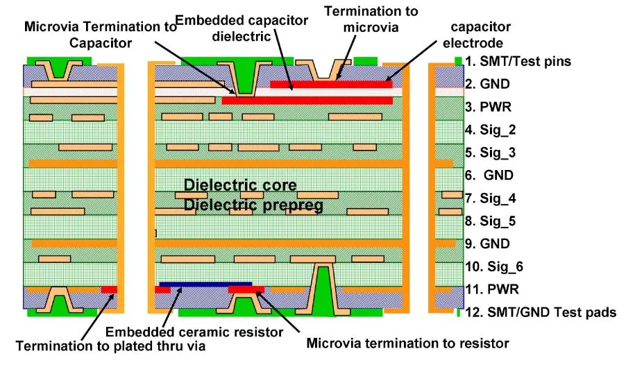
2. Via-in-Pad Filling and Capping Requirements
The customer explicitly required all via-in-pad (under BGA) to be resin filled and capped on both sides. Our CAM team identified that some vias had very small annular rings, making reliable filling and capping challenging. We recommended filling and capping all vias in the BGA area, including different hole sizes (0.15 mm, 0.2 mm, 0.25 mm), to ensure consistent planar surface for BGA soldering.
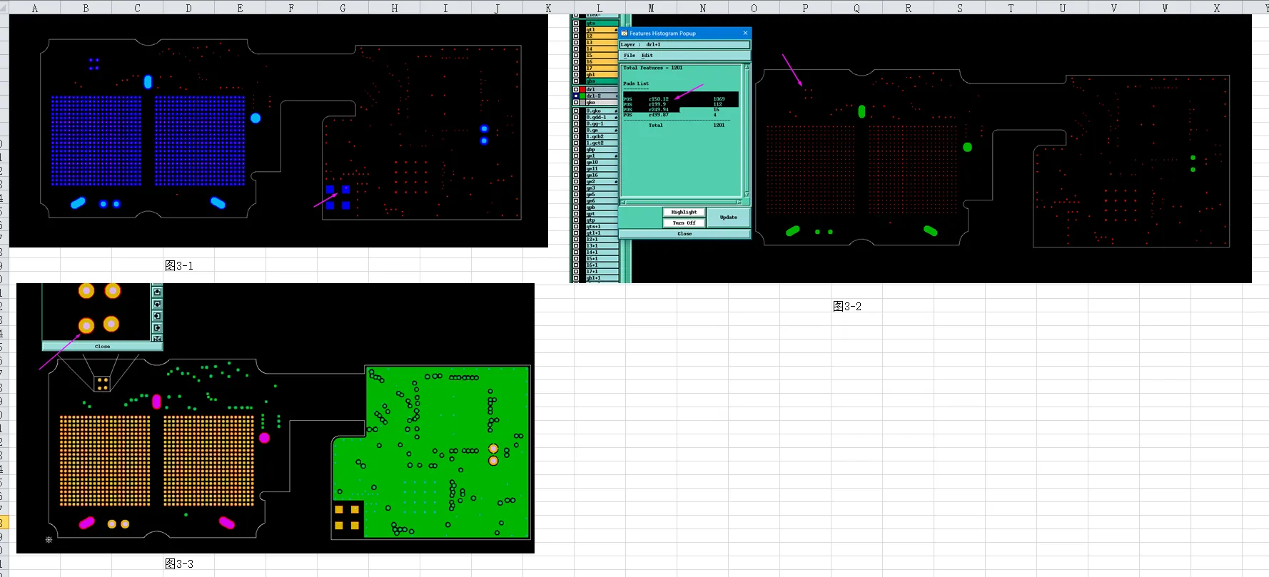
Figure 2: filling and capping all vias in the BGA area
We noticed that following the original data strictly could leave some vias unfilled, leading to solder wicking into the holes during assembly. If not properly addressed, this would cause poor solder joint reliability, head-in-pillow defects, or BGA component failures after thermal cycling.
According to typical IPC-6012 Class 2/3 requirements for via filling, complete filling and capping are essential for high-reliability BGA applications to prevent voids and ensure flatness.
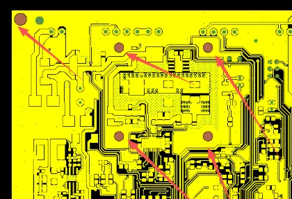
3. Flex-Rigid Transition Zone and Via Movement
In the flex-rigid transition area, several vias were too close to the flex zone boundary. To reduce the risk of chemical intrusion and delamination, our engineering team moved affected vias by 0.6 mm and adjusted corresponding pads and traces.
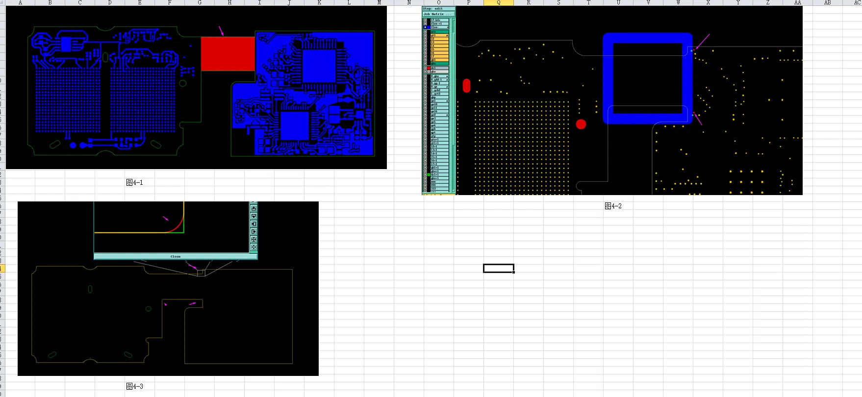
Figure 3: several vias were too close to the flex zone boundary
We also changed sharp inner corners in the flex outline to 0.5 mm radius to prevent tearing during bending. Additionally, we added independent copper pads on inner layers in the transition zone to improve layer adhesion.
If these adjustments had not been made, vias near the flex area could allow plating chemicals to penetrate inner layers, causing contamination, short circuits, or complete board scrap. The sharp corners would increase the likelihood of flex material tearing during assembly or use.
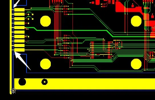
4. Solder Mask Optimization and Slot Hole Manufacturing
We optimized solder mask openings to maintain 1-2 mil clearance around pads while preserving solder mask bridges between pads. An ultra-short slot hole (1.0 x 1.1 mm) was converted to a round 1.1 mm hole as it could not be reliably produced.
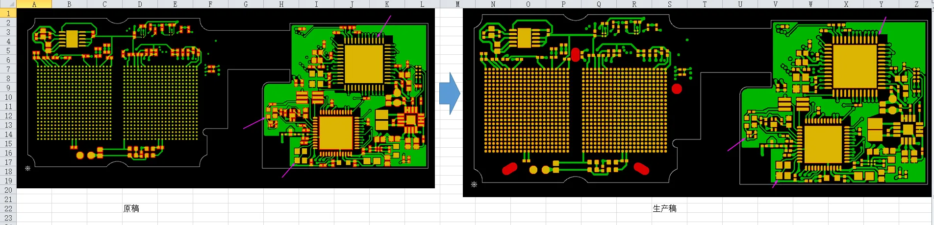
Figure 4: optimized solder mask openings
Our engineer also confirmed flex coverlay material (yellow) and rigid solder mask (green, no silkscreen).
Manufacturing Risks and DFM Insights
Rigid-flex designs frequently trigger EQs due to the different processing requirements of rigid and flex sections. Common pitfalls include unclear stackup documentation, insufficient via-in-pad specifications, and inadequate consideration of the transition zone. These issues can lead to delamination, via reliability problems, and flex tearing if not caught early.
The via-in-pad requirement was particularly critical here. Without proper filling and capping, BGA assembly yield would drop significantly due to solder voids and uneven surfaces.
How the Engineering Team Resolved the Issues
Our team provided multiple updated production files and annotated drawings throughout the review process. We optimized the stackup, adjusted via positions in the transition area, implemented full via-in-pad filling where needed, and refined outline features for better manufacturability. All changes were sent for customer confirmation before final release.
Final Manufacturing Outcome
All engineering questions were resolved after iterative clarifications. The stackup was optimized and approved, via-in-pad processing confirmed, transition zone adjustments accepted, and production files finalized. The order was released for fabrication with updated manufacturing parameters.
Key Takeaways for PCB Designers
- Provide clear, detailed stackup drawings that specify copper weights for both rigid and flex sections.
- Clearly define via-in-pad requirements, including filling and capping, especially under BGA components.
- Maintain adequate clearance between vias and flex-rigid transition zones to prevent chemical intrusion.
- Use rounded corners (minimum 0.5 mm) in flex outline areas to reduce tearing risk.
- Verify slot hole dimensions early - ultra-short slots are often impossible to produce reliably.
- Ensure solder mask and coverlay data are consistent with pad sizes for reliable soldering.
- Consider adding adhesion-enhancing features like independent pads in transition zones.
FAQ
Q1: Why is via-in-pad filling and capping critical for BGA areas?
A1: Unfilled vias can cause solder to wick into the hole during reflow, resulting in insufficient solder volume, voids, and unreliable BGA joints that may fail under thermal or mechanical stress.
Q2: What are the main challenges in rigid-flex stackup design?
A2: Balancing copper thickness for both bendability in flex areas and rigidity in component sections, while ensuring reliable lamination at the transition zone.
Q3: Why move vias away from the flex-rigid junction?
A3: Vias too close to the flex area risk allowing chemicals to penetrate inner layers during processing, which can cause contamination, shorts, or delamination.
Q4: Can ultra-short slot holes be manufactured as designed?
A4: No. Very short slots (aspect ratio too extreme) are difficult to produce cleanly and are often converted to round holes to ensure manufacturing feasibility and quality.
Q5: What causes delamination in rigid-flex PCBs?
A5: Common causes include mismatched materials, insufficient adhesion features in transition zones, or chemical exposure at the junction during processing.