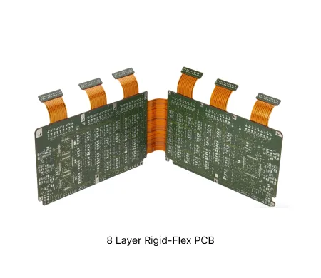
PCB Specifications
| Parameter | Value | Parameter | Value |
|---|---|---|---|
| PCB Type | Rigid-Flex PCB | Quantity | 5 pcs |
| Layers | 8 Layers | Board Type | Panel PCB |
| Dimensions | 21.8 x 58.11 mm | Copper Weight | 1OZ |
| Thickness | 1 mm | Min Track / Spacing | 4/4mil |
| Surface Finish | ENIG (Immersion Gold) | Min Hole Size | 0.15mm |
| Solder Mask | Green | Silkscreen | None |
Manufacturing Timeline
Logistics Information
Key Manufacturing Processes
Manufacturing Summary
This order involved the fabrication of a rigid-flex PCB consisting of an 8-layer rigid section (1.0 mm thick, Shengyi S1150G, TG155, 1 oz copper) bonded to a flexible section (Shengyi SF305C polyimide with double-sided yellow coverlay). The design featured fine geometry with 4 mil line/space, 0.15 mm minimum holes, backdrilling, and a high-density BGA area requiring via-in-pad structures to be fully resin plugged and capped on both sides. Boards were panelized 1×5 with process edges, positioning holes, and fiducials, finished in ENIG (1.0 µ″ Au), and tested via 100% flying probe. The combination of rigid-flex construction, via-in-pad resin processing under BGA, and tight mechanical/electrical requirements made this a technically demanding build.
During engineering review, several DFM points required clarification and optimization. Some vias were initially too close to the flex zone (< 0.6 mm), creating risk of chemical ingress during processing; these were relocated with corresponding pad and trace adjustments. Sharp inner corners at the rigid-flex transition were changed to R0.5 mm fillets to reduce tearing risk during flexing. Independent bonding pads were added on inner layers to improve adhesion. The ultra-short slot (1.0 × 1.1 mm) was converted to a round hole for manufacturability. BGA via-in-pad features (including the disk-in-hole) received complete resin plugging and capping on both sides, while solder mask openings were standardized to 1–2 mil larger than pads with retained bridges. Stackup and copper weights were aligned (inner layers 0.5 oz, outer 1 oz) to balance producibility and bendability, and BGA pad sizes plus routing were optimized to mitigate lift-off risk. All changes were confirmed through iterative production file updates.
With these adjustments implemented and materials/processes verified, the panels were processed successfully, meeting the specified rigid board thickness (1.0 ± 0.1 mm), flex stackup, and surface finish requirements. The proactive handling of via clearance, transition geometry, via-in-pad plugging, and fine-feature optimizations ensured structural integrity and reliable BGA performance.
Explore More PCB Manufacturing Resources
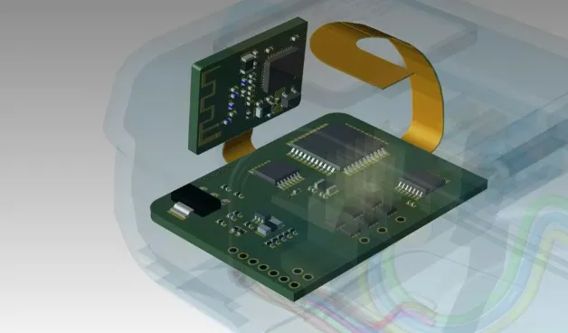
8 Layer Rigid-Flex PCB Manufacturing Insights
These boards combine multiple rigid zones with flexible interconnects. The construction supports complex routing in space-constrained dynamic applications.
The Ultimate Guide to Rigid-Flex PCB Design: Mastering Reliability, Complexity, and Cost
Master the complexities of Rigid-Flex PCB Design with this 2,500-word guide. Explore stack-up symmetry, bend radius calculations, via optimization, and cost-effective manufacturing strategies.
Real Production Records
| Order ID | PCB Type | Layers | Dimensions | Solder Mask | Surface Finish | Quantity | Action |
|---|---|---|---|---|---|---|---|


