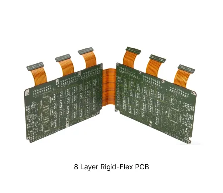
Typical Specification Range
| Parameter | Standard parameters for 8 layer rigid-flex designs |
|---|---|
| Layer count | 8 layers |
| Material type | FR-4 rigid, Polyimide flex |
| Surface finish | ENIG, Immersion Silver, OSP |
| Thickness | 0.8-2.5 mm |
| Solder mask | LPI on rigid, green. Coverlay on flex, yellow, white |
| Copper thickness | 0.5 oz to 2 oz |
| Special features | Blind buried vias, impedance control, stiffeners |
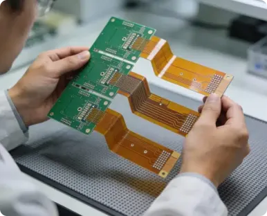
Manufacturing Process Insights
Sequential Lamination
Multiple press cycles bond rigid cores to flex layers. Precise temperature and pressure profiles prevent material flow into flex zones.
Drilling and Plating
Laser and mechanical drilling create microvias. Copper plating ensures reliable vertical interconnects across all 8 layers.
Surface Finish Application
ENIG is applied selectively to rigid areas. This protects pads while maintaining flex region flexibility.
Risk Control
Special fixtures control registration at transitions. Cross-section analysis verifies plating thickness and material integrity.
Manufacturing Order Profile
| Order Quantity | Order Proportion | Estimated Price Level | Typical Lead Time |
|---|---|---|---|
| Prototype (<=30 pcs) | 78% | From $782 | From 22 days |
| Small volume (30-200 pcs) | 17% | From $986 | From 24 days |
| Mass production (>200 pcs) | 5% | From $1667 | From 26 days |
Manufacturing Challenges & Process Optimization
Design Considerations
Related Products
.webp)
Common Applications
PCB Solution for Consumer Electronics
AIVON's consumer electronics PCBs are precision-engineered for smartphones, tablets, laptops, and smart home devices. Using HDI design, fine-line etching, and multilayer fabrication, they deliver compact layouts, high-speed signal transmission, and strong reliability while meeting international quality and environmental standards.
PCB Solution for Aerospace and Aviation
AIVON provides high-reliability PCBs designed for civil aviation and aerospace applications, built to perform under extreme conditions such as vibration, temperature variation, and high-altitude environments. These PCBs are widely used in avionics systems, flight control modules, communication equipment, and satellite technologies. With advanced multilayer structures, heavy copper options, and high-temperature materials, our solutions are engineered to meet stringent reliability standards such as IPC-6012 Class 3.
PCB Solution for Medical Devices
AIVON medical device PCBs are high-reliability boards designed for healthcare applications. Built with strict quality control, biocompatible materials, and precise manufacturing, they ensure safety and accuracy. Suitable for diagnostic equipment, patient monitoring, and wearable medical devices, AIVON PCBs meet ISO and IPC medical standards.
Real Production Records
| Order ID | PCB Type | Layers | Dimensions | Solder Mask | Surface Finish | Quantity | Action |
|---|---|---|---|---|---|---|---|
| Loading... | |||||||
View More Engineering Resources
Why Choose AIVON for 8 Layer Rigid-Flex PCB?
AIVON produces 8 layer rigid-flex PCBs with precise multi-layer registration, controlled impedance, and reliable plated through holes across rigid and flex zones. We maintain tight tolerances on dielectric thickness, transition areas, bend radius, and overall board thickness while ensuring strong lamination bonding and consistent copper plating. This delivers superior signal integrity and mechanical durability for complex, high-density applications in medical, aerospace, and automotive systems.
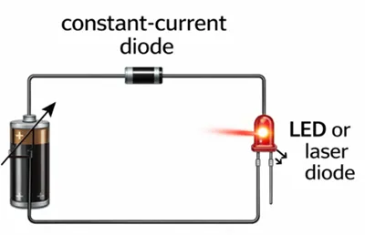
Current Limiter: Usage and Operating Principle
Technical overview of current limiters: uses, circuit principles, filtering and EMC concerns, and practical methods to adjust, bypass, or disable current limiting.
Read More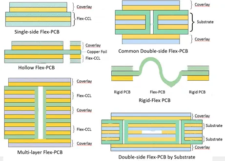
Sequential Lamination for Rigid-Flex PCBs: Design Considerations and Manufacturing Challenges
Rigid flex PCB design rules address sequential lamination challenges in flexible PCB manufacturing. This guide covers technical principles, stackup planning, transition zones, best practices, troubleshooting, and FAQs for reliable production and performance.
Read More


