Typical Specification Range
| Parameter | Typical Range |
|---|---|
| Layer count | 8 layers |
| Material type | High Tg FR-4, low loss laminates |
| Surface finish | ENIG, Immersion Silver, OSP |
| Thickness | 0.8 mm to 3.0 mm |
| Solder mask | Liquid photoimageable, green or black |
| Copper thickness | 0.5 oz to 2 oz |
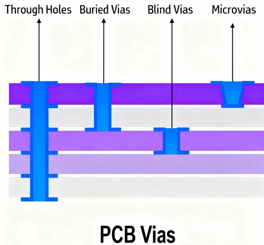
| Special features | Blind vias, buried vias, stacked microvias, impedance control, via-in-pad, sequential lamination |
Manufacturing Process Insights
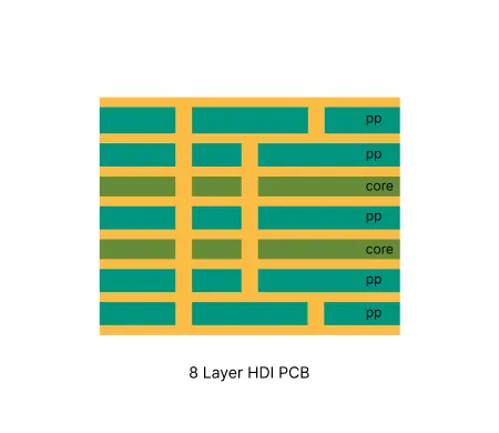
Sequential Lamination: Multiple press cycles build the 8 layer structure with tight registration control.
Laser Drilling: UV or CO2 lasers create microvias. Desmear removes resin smear before plating.
Copper Plating: Pulse plating ensures uniform deposition in high aspect ratio microvias.
Surface Finish: ENIG is selected for fine pitch assembly compatibility. Process monitoring prevents delamination and controls warpage throughout fabrication.
Manufacturing Order Profile
| Order Quantity | Order Proportion | Estimated Price Level | Typical Lead Time |
|---|---|---|---|
| Prototype (<=30 pcs) | 71% | From $250 | From 9 days |
| Small volume (30-200 pcs) | 23% | From $280 | From 9 days |
| Mass production (>200 pcs) | 6% | From $400 | From 10 days |
Manufacturing Challenges & Process Optimization
Design Considerations
Related Products
.webp)
Common Applications
PCB Solution for Aerospace and Aviation
AIVON provides high-reliability PCBs designed for civil aviation and aerospace applications, built to perform under extreme conditions such as vibration, temperature variation, and high-altitude environments. These PCBs are widely used in avionics systems, flight control modules, communication equipment, and satellite technologies. With advanced multilayer structures, heavy copper options, and high-temperature materials, our solutions are engineered to meet stringent reliability standards such as IPC-6012 Class 3.
PCB Solution for Automotive Electronics
AIVON automotive electronics PCBs are designed for demanding vehicle environments. They withstand extreme temperatures, vibration, and harsh conditions, supporting ECUs, ADAS, infotainment, and EV modules. Featuring multilayer, rigid-flex, and high-frequency designs, AIVON PCBs meet IATF 16949 standards for safe and reliable automotive performance.
PCB Solution for New Energy
AIVON empowers the renewable sector with high-performance PCBs for solar inverters, wind turbines, and Battery Management Systems (BMS). Engineered to withstand high voltages and harsh outdoor environments, our boards ensure precise energy conversion. Maximize your energy harvest and storage efficiency with our reliable, robust interconnect solutions.
Real Production Records
| Order ID | PCB Type | Layers | Dimensions | Solder Mask | Surface Finish | Quantity | Action |
|---|---|---|---|---|---|---|---|
| Loading... | |||||||
View More Engineering Resources
Why Choose AIVON for 8 Layer HDI PCB?
Need reliable 8 Layer HDI PCB production? AIVON supports multi-stage sequential lamination, laser microvias, and tight registration control, delivering stable impedance, strong stacked via reliability, and consistent high-yield output for volume builds.
Stacked Vias in HDI PCBs: Design, Manufacturing, and Reliability
Explore stacked vias in High-Density Interconnect (HDI) PCBs, covering their design principles, manufacturing processes, key reliability considerations, and cost implications.
Read More
Advanced HDI PCB Stackup Materials for Improved Signal Performance
Explore advanced HDI PCB stackup materials for enhanced signal performance. Learn about low Dk, low loss, high Tg, and impedance control materials.
Read More


