Typical Specification Range
| Parameter | Typical Range |
|---|---|
| Layer count | 4 layers |
| Material type | FR4 TG130 to TG170 |
| Surface finish | HASL, ENIG, OSP |
| Thickness | 0.8mm - 1.6mm |
| Solder mask | Green, black, red, white, yellow, blue, purple, matte black, matte black |
| Copper thickness | 1oz - 8oz |
| Special features | Impedance control, via plugging, heavy copper, gold fingers |
Manufacturing Process Insights
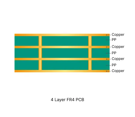
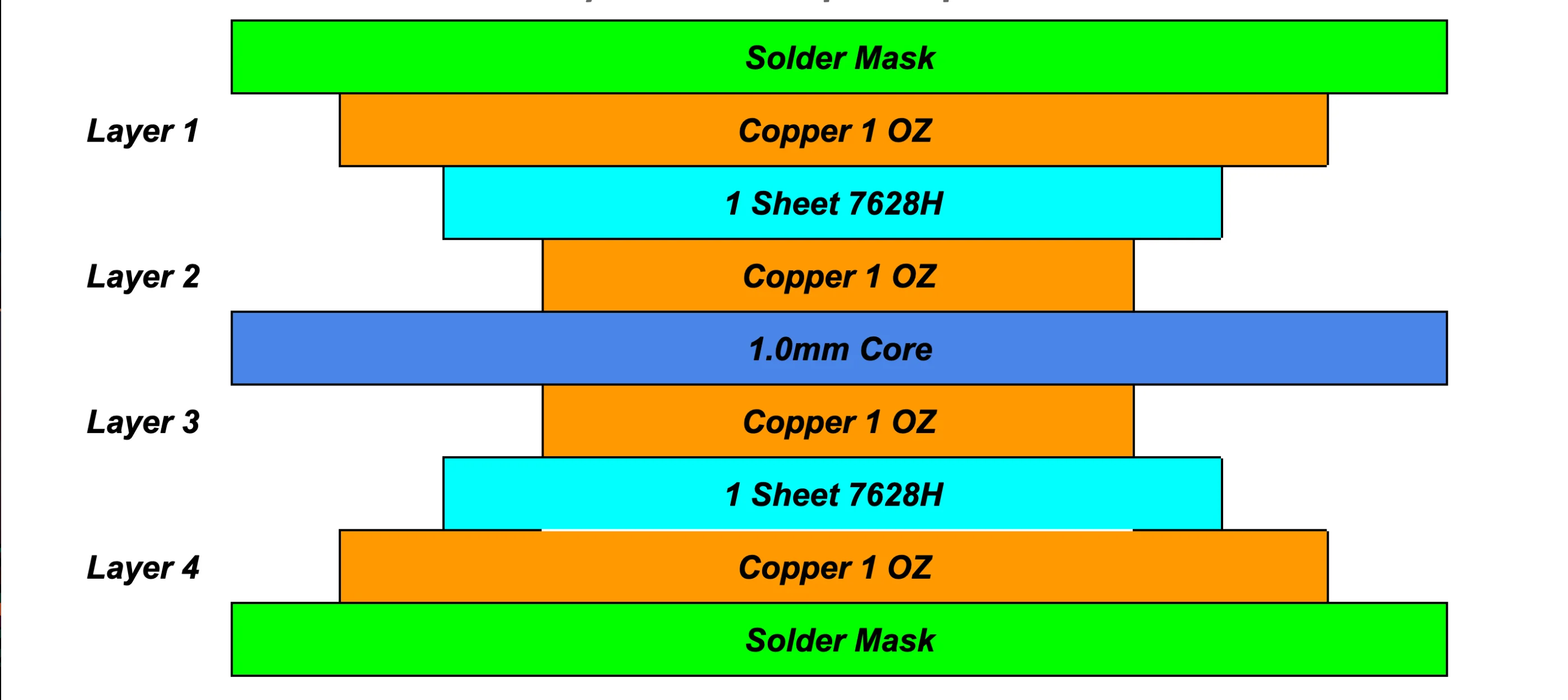
4 layer FR4 PCBs begin with inner layer imaging, etching, and oxide treatment. Core and prepreg sheets are stacked then laminated under controlled heat and pressure.
Precision drilling creates through vias. Electroless copper plating establishes interlayer connections before pattern plating and etching.
Surface finish is applied according to assembly requirements and shelf life needs. Final routing and electrical testing complete the process.
Registration accuracy during lamination receives close attention. Drill quality and plating uniformity directly determine via reliability.
Manufacturing Order Profile
| Order Quantity | Order Proportion | Estimated Price Level | Typical Lead Time |
|---|---|---|---|
| Prototype (<=30 pcs) | 55% | From $1 | From 2 days |
| Small volume (30-200 pcs) | 30% | From $70 | From 2 days |
| Mass production (>200 pcs) | 15% | From $140 | From 3 days |
Manufacturing Challenges & Process Optimization
Design Considerations
Related Products
.webp)
Common Applications
PCB Solution for Medical Devices
AIVON medical device PCBs are high-reliability boards designed for healthcare applications. Built with strict quality control, biocompatible materials, and precise manufacturing, they ensure safety and accuracy. Suitable for diagnostic equipment, patient monitoring, and wearable medical devices, AIVON PCBs meet ISO and IPC medical standards.
PCB Solution for Automotive Electronics
AIVON automotive electronics PCBs are designed for demanding vehicle environments. They withstand extreme temperatures, vibration, and harsh conditions, supporting ECUs, ADAS, infotainment, and EV modules. Featuring multilayer, rigid-flex, and high-frequency designs, AIVON PCBs meet IATF 16949 standards for safe and reliable automotive performance.
PCB Solution for Consumer Electronics
AIVON's consumer electronics PCBs are precision-engineered for smartphones, tablets, laptops, and smart home devices. Using HDI design, fine-line etching, and multilayer fabrication, they deliver compact layouts, high-speed signal transmission, and strong reliability while meeting international quality and environmental standards.
Real Production Records
| Order ID | PCB Type | Layers | Dimensions | Solder Mask | Surface Finish | Quantity | Action |
|---|---|---|---|---|---|---|---|
| Loading... | |||||||
View More Engineering Resources
Why Choose AIVON for 4 Layer FR4 PCB?
AIVON specializes in 4 Layer FR4 PCB manufacturing with precise multilayer alignment, controlled lamination pressure, and strict impedance control, ensuring consistent electrical performance, high via reliability, and stable mass production yield.
4 Layer PCB Stack Up: A Practical Tutorial for Simple Designs
This tutorial covers 4-layer PCB stackup basics for simple hobby designs, including layer arrangements, ground and power planes, symmetry to avoid warpage, signal integrity tips, and troubleshooting. Follow best practices for reliable prototypes with standards like IPC-2221C.
Read More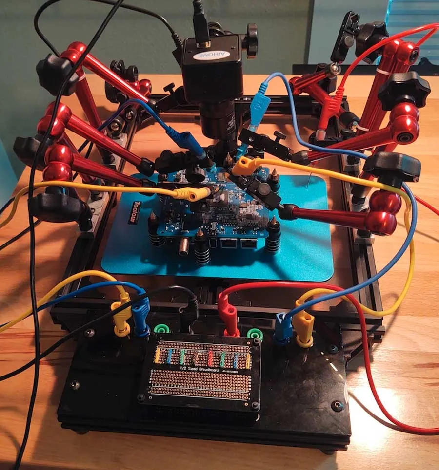
Building Your Own PCB Test Setup: A Comprehensive DIY Guide for Hobbyists and Engineers
Learn how to build a DIY PCB test setup with pogo pins, Arduino automation, and step-by-step jig instructions. Perfect for hobbyists and engineers—create a professional-grade homemade tester under $100 and diagnose faults fast.
Read More


