Introduction
For electronic hobbyists stepping up from basic two-layer boards, a 4-layer PCB design offers a straightforward way to improve performance without overwhelming complexity. This PCB stackup configuration adds dedicated planes for power and ground, which helps manage noise and signal integrity in simple circuits like microcontrollers, sensors, or audio amplifiers. Understanding the PCB layer stack becomes essential as projects grow, allowing better routing and reduced electromagnetic interference. This tutorial breaks down the fundamentals of 4-layer PCB stackup for beginners, focusing on practical choices that keep costs low and fabrication reliable. By following a logical approach, hobbyists can create robust boards that perform well in prototypes and small productions.
4-Layer PCB Design Guide: Optimizing Your PCB Stackup for Signal Integrity
A PCB stackup refers to the precise arrangement of conductive copper layers and insulating dielectric materials in a multilayer board. In a 4-layer PCB design, this typically includes two outer signal layers and two inner planes, often dedicated to ground and power distribution. This setup contrasts with two-layer boards by providing continuous reference planes that shorten return paths for signals, minimizing crosstalk and inductance. For hobbyists working on simple designs, such as Arduino shields or LED drivers, the PCB layer stack matters because it simplifies routing high-speed traces and ensures stable power delivery. Without proper stackup planning, boards can suffer from ground loops or excessive noise, leading to erratic behavior in sensitive components. Adhering to guidelines from IPC-2221C helps achieve a balanced structure that supports reliable operation.
The relevance grows as hobby projects incorporate faster microprocessors or mixed analog-digital signals. A well-planned PCB stackup reduces the need for complex shielding and allows components to fit on smaller footprints. Hobbyists benefit from lower EMI emissions, which is crucial for passing basic compliance tests or avoiding interference in home labs. Moreover, standard 4-layer configurations keep manufacturing straightforward, with most services offering predefined options. This accessibility makes transitioning to 4-layer boards a practical next step in a PCB design guide.
Core Principles of PCB Stackup and Layer Sequencing in 4-Layer PCB Design
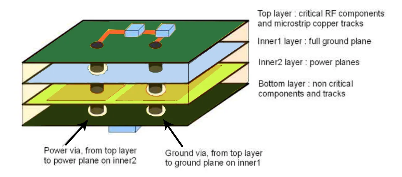
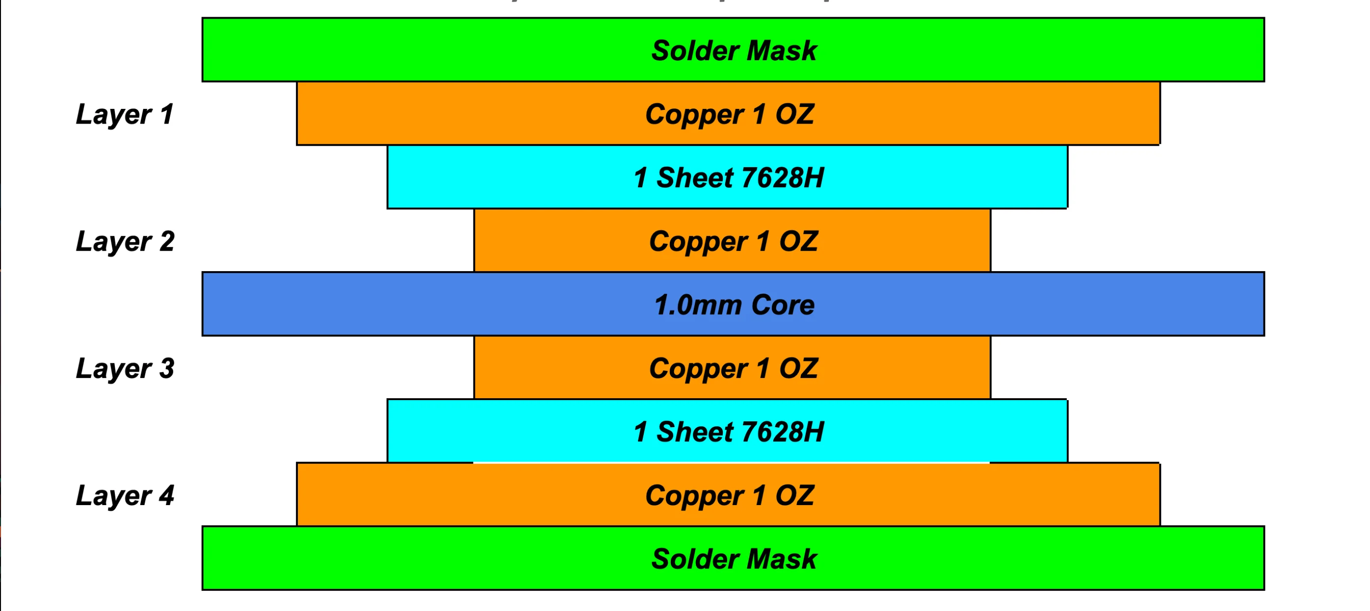
The core principle of any PCB stackup lies in layering copper foils with prepregs and cores, bonded under heat and pressure to form a rigid structure. In 4-layer boards, the sequence usually starts with a top signal layer for components and traces, followed by a ground plane, a power plane, and a bottom signal layer. Dielectric thicknesses between layers control impedance and capacitance, while symmetry from top to bottom prevents warpage during fabrication. Copper weight, typically uniform across layers, influences current-carrying capacity and thermal dissipation. Vias connect layers, with through-hole types common in simple designs due to their ease of implementation.
Signal integrity improves because adjacent planes provide low-inductance return paths, confining fields between layers. For instance, placing ground directly under the top signal layer creates a stripline-like environment for controlled impedance traces. Power planes distribute voltage evenly, reducing voltage drops across the board. Material selection focuses on FR-4 for cost-effectiveness, with its dielectric constant affecting signal speed. IPC-2221C outlines requirements for layer sequencing to optimize these interactions, ensuring mechanical stability.
Thermal management also plays a role, as inner planes act as heat spreaders. Uneven copper distribution can cause bowing, so balanced stackups maintain flatness. Aspect ratios for vias must consider drill-to-board thickness to avoid plating voids. These principles form the foundation of effective 4-layer PCB design, guiding hobbyists toward predictable results.
Related Reading: Routing Simple Circuits on a 4 Layer PCB: A Practical Approach
1.6 mm PCB Stackup Best Practices: A Practical 4-Layer PCB Design Guide
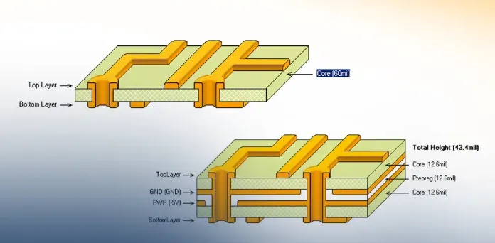
Start with a standard PCB stackup for 1.6 mm total thickness, which most fabricators support without custom tooling. Assign the inner layers as full ground and power planes to maximize their utility in simple circuits. Route critical signals on outer layers adjacent to their reference planes, keeping traces short and avoiding splits in planes under high-speed lines. Use ground vias liberally near signal vias to provide stitching and low-impedance paths. This configuration supports 50-ohm impedance for common hobbyist signals without advanced calculations.
Symmetry is key: match dielectric thicknesses above and below the core to minimize stress during lamination. Pour power and ground planes as solid as possible, with clearance for voltage isolation following safety margins. For mixed-signal boards, split the ground plane only if necessary, and connect splits with narrow bridges or capacitors. Blind or buried vias are rarely needed in simple designs, sticking to through vias keeps costs down. Always verify stackup against fabrication capabilities early in the PCB design guide.
Impedance control, while optional for low-speed hobby projects, becomes achievable by adjusting trace width and dielectric spacing. Ground the unused portions of power planes to enhance shielding. Test prototypes for continuity and shorts before assembly. These practices align with IPC-6012F performance specs, ensuring boards meet basic quality thresholds.
Related Reading: Power and Ground Plane Design in 4 Layer PCBs
Common 4-Layer PCB Design Configurations and Troubleshooting Your PCB Layer Stack
Two primary 4-layer configurations suit simple designs: the signal-ground-power-signal stack for general use, and signal-power-ground-signal for power-heavy applications. The first excels in digital circuits by sandwiching signals between planes, reducing radiation. Hobbyists often choose the former for its EMI suppression. Variations depend on component density and voltage rails.
Troubleshooting starts with warpage, caused by asymmetric stackups or CTE mismatches. Inspect for bowing using a flat surface and feeler gauges; rework by symmetrizing layers. Signal crosstalk appears as noise on scopes; mitigate by tightening plane adjacency. Power integrity issues like ripple stem from plane splits; consolidate pours. Fabricators provide stackup drawings for verification.
For hobbyists, simulate routing mentally: outer layers for parts and buses, inners for planes. Document the PCB layer stack clearly in Gerber files.
Conclusion
Mastering 4-layer PCB stackup empowers hobbyists to build more capable boards with confidence. Key takeaways include prioritizing plane adjacency, ensuring symmetry, and leveraging standards for reliability. This approach enhances signal quality and simplifies layout in a PCB design guide. Start with standard configurations, iterate based on prototypes, and scale to complex projects gradually. Reliable 4-layer designs elevate hobby work to professional levels without excessive cost.
FAQs
Q1: What is a typical PCB stackup for a 4-layer PCB design?
A1: A common PCB stackup places signal layers on top and bottom, with inner ground and power planes. This setup provides reference planes for signals, aiding impedance control and noise reduction. For simple hobbyist circuits, use uniform dielectric thicknesses for symmetry. Fabricators often supply predefined options matching this configuration.
Q2: Why choose a 4-layer over 2-layer PCB layer stack?
A2: A 4-layer PCB layer stack offers dedicated planes, improving power distribution and EMI shielding for denser routing. Hobbyists benefit from easier high-speed signal handling without extra shielding. It supports more components on smaller boards while maintaining performance.
Q3: How does PCB stackup affect signal integrity in 4-layer designs?
A3: PCB stackup influences return paths and coupling; adjacent planes minimize inductance for clean signals. In 4-layer PCB design, ground under signal layers confines fields, reducing crosstalk. Proper via placement enhances integrity for hobby projects.
Q4: What are best practices for 4-layer PCB stackup symmetry?
A4: Balance dielectric thicknesses top-to-bottom to prevent warpage during lamination. Use matching copper weights across layers. This follows IPC guidelines, ensuring flat boards for reliable assembly in simple designs.
References
IPC-2221C — Generic Standard on Printed Board Design. IPC, 2023
IPC-6012F — Qualification and Performance Specification for Rigid Printed Boards. IPC, 2023
IPC-A-600K — Acceptability of Printed Boards. IPC, 2020


