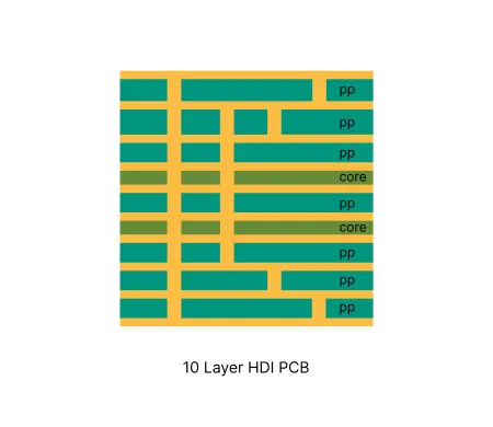
Typical Specification Range
| Parameter | High density interconnect boards using microvias and sequential build-up |
|---|---|
| Layer count | 10 layers |
| Material type | High Tg FR-4, low Dk laminates |
| Surface finish | ENIG, ENEPIG, Immersion Silver |
| Thickness | 0.8-2.5 mm |
| Solder mask | Green, black, red, white, yellow, purple, matte black |
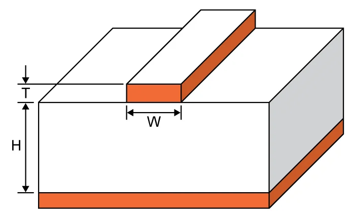
| Copper thickness | 0.5-2 oz |
| Special features | Blind microvias, buried vias, stacked vias, fine line routing |
Manufacturing Process Insights
Sequential Lamination: Core and prepreg materials are pressed in multiple cycles to build 10 layers with accurate registration.
Laser Drilling: UV or CO2 lasers create microvias. Plasma desmear prepares surfaces for plating.
Plating and Surface Finish: Copper electroplating fills vias. ENIG finish protects pads and ensures assembly compatibility.
Process controls focus on registration management, plating uniformity, and thermal stress reduction to maintain yield.
Manufacturing Order Profile
| Order Quantity | Order Proportion | Estimated Price Level | Typical Lead Time |
|---|---|---|---|
| Prototype (<=30 pcs) | 44% | From $328 | From 8 days |
| Small volume (30-200 pcs) | 35% | From $368 | From 10 days |
| Mass production (>200 pcs) | 21% | From $504 | From 10 days |
Manufacturing Challenges & Process Optimization
Design Considerations
Related Products
Common Applications
PCB Solution for Telecommunication
AIVON telecommunication PCBs are high-performance boards designed for fast and stable signal transmission. Used in base stations, routers, satellite systems, and 5G infrastructure, they feature advanced materials and precision manufacturing to ensure low signal loss, accurate impedance control, and reliable high-frequency performance.
PCB Solution for Medical Devices
AIVON medical device PCBs are high-reliability boards designed for healthcare applications. Built with strict quality control, biocompatible materials, and precise manufacturing, they ensure safety and accuracy. Suitable for diagnostic equipment, patient monitoring, and wearable medical devices, AIVON PCBs meet ISO and IPC medical standards.
PCB Solution for Consumer Electronics
AIVON's consumer electronics PCBs are precision-engineered for smartphones, tablets, laptops, and smart home devices. Using HDI design, fine-line etching, and multilayer fabrication, they deliver compact layouts, high-speed signal transmission, and strong reliability while meeting international quality and environmental standards.
Real Production Records
| Order ID | PCB Type | Layers | Dimensions | Solder Mask | Surface Finish | Quantity | Action |
|---|---|---|---|---|---|---|---|
| Loading... | |||||||
View More Engineering Resources
Why Choose AIVON for 10 Layer HDI PCB?
AIVON manufactures 10 Layer HDI PCBs with advanced microvia technology and precise laser drilling for high-density interconnects. Strict multilayer lamination, accurate registration control, and reliable copper plating ensure excellent interlayer alignment, tight impedance control, and superior reliability in compact, high-performance applications.
Advanced RF PCB Routing Techniques: Mastering Microstrips and Striplines
Learn advanced RF PCB routing techniques for microstrip and stripline designs. Gain practical insights on impedance control and signal integrity to improve high frequency performance in your PCB layouts.
Read More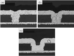
Troubleshooting Common HDI PCB Problems: A Practical Guide
Learn practical solutions with this HDI PCB troubleshooting guide. Identify and fix common defects like microvia failures and signal issues. Perfect for electrical engineers seeking reliable failure analysis tips.
Read More


