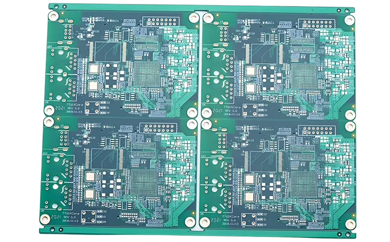
Typical Specification Range
| Parameter | ENIG finished boards for HDI applications |
|---|---|
| Layer count | 4-20 layers |
| Material type | High Tg FR-4, low loss laminates |
| Surface finish | ENIG |
| Thickness | 0.8-3.0 mm |
| Solder mask | Green, black, red, white, matte black |
| Copper thickness | 0.5 oz to 2 oz |
| Special features | Microvias, stacked vias, via-in-pad, fine lines |
Manufacturing Process Insights
Sequential Lamination: Build HDI layers with tight registration between laser drilled microvias.
Drilling: Combine UV laser for microvias and mechanical drilling for through holes.
Plating: Apply direct metallization followed by copper electroplating with strong throwing power.
ENIG Surface Finish: Deposit electroless nickel then immersion gold after solder mask.
9975
Risk Control: Monitor bath chemistry to prevent black pad and ensure uniform plating thickness.
Manufacturing Order Profile
| Order Quantity | Order Proportion | Estimated Price Level | Typical Lead Time |
|---|---|---|---|
| Prototype (<=30 pcs) | 69% | From $208 | From 8 days |
| Small volume (30-200 pcs) | 22% | From $242 | From 9 days |
| Mass production (>200 pcs) | 9% | From $355 | From 9 days |
Manufacturing Challenges & Process Optimization
Design Considerations
Related Products
Common Applications
PCB Solution for Consumer Electronics
AIVON's consumer electronics PCBs are precision-engineered for smartphones, tablets, laptops, and smart home devices. Using HDI design, fine-line etching, and multilayer fabrication, they deliver compact layouts, high-speed signal transmission, and strong reliability while meeting international quality and environmental standards.
PCB Solution for Telecommunication
AIVON telecommunication PCBs are high-performance boards designed for fast and stable signal transmission. Used in base stations, routers, satellite systems, and 5G infrastructure, they feature advanced materials and precision manufacturing to ensure low signal loss, accurate impedance control, and reliable high-frequency performance.
PCB Solution for Medical Devices
AIVON medical device PCBs are high-reliability boards designed for healthcare applications. Built with strict quality control, biocompatible materials, and precise manufacturing, they ensure safety and accuracy. Suitable for diagnostic equipment, patient monitoring, and wearable medical devices, AIVON PCBs meet ISO and IPC medical standards.
Real Production Records
| Order ID | PCB Type | Layers | Dimensions | Solder Mask | Surface Finish | Quantity | Action |
|---|---|---|---|---|---|---|---|
| Loading... | |||||||
View More Engineering Resources
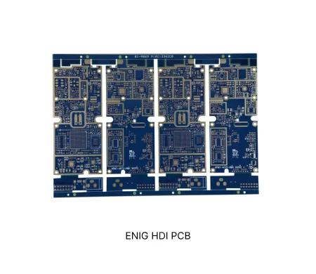
Why Choose AIVON for ENIG HDI PCB?
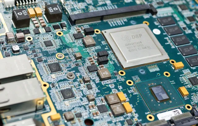
AIVON produces ENIG HDI PCBs with precise laser drilling for microvias and uniform ENIG surface finish for excellent solderability and flatness. Strict multilayer lamination, accurate registration, and reliable copper plating ensure tight impedance control, high reliability, and superior performance in high-density, fine-pitch SMT applications.
The Role of HDI PCBs in Telecommunication Base Stations: Benefits and Design Considerations
HDI PCBs enable compact telecommunication base stations through high-density interconnect features and base station PCB miniaturization. Microvias PCB and fine-pitch PCB designs improve signal integrity and routing density. This article outlines key benefits, technical principles, design considerations, and standards for reliable performance in 5G applications.
Read More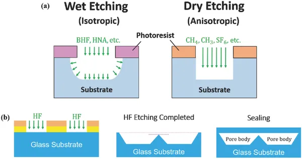
Advanced PCB Etching Techniques for High Density Interconnect (HDI) Boards
HDI PCB etching techniques achieve fine line precision in high-density interconnect boards. Details on semi-additive processes, plasma etching, LDI imaging, best practices, and troubleshooting for reliable manufacturing. Insights for electric engineers on standards compliance and high yields in compact designs. (178 characters)
Read More


