Introduction
Telecommunication base stations form the backbone of modern wireless networks, handling vast amounts of data at high speeds. As networks evolve toward 5G and beyond, the demand for compact, high-performance electronics intensifies. HDI PCBs, or high-density interconnect printed circuit boards, play a pivotal role in meeting these requirements by enabling denser component integration. These boards support the miniaturization essential for base stations deployed in urban environments with limited space. Engineers designing such systems must understand how HDI technology addresses signal integrity, thermal challenges, and reliability under continuous operation. This article explores the benefits and key design considerations for HDI PCBs in telecommunication base stations.
What Are HDI PCBs?
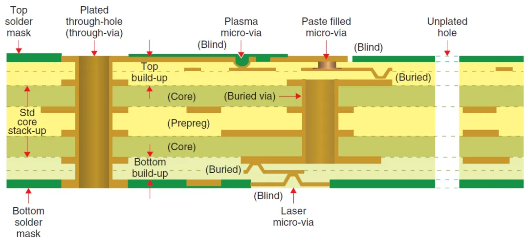
HDI PCBs represent an advanced evolution of traditional multilayer boards, characterized by finer features and innovative via structures. High-density interconnect technology incorporates microvias, which are smaller than standard through-holes, typically formed by laser drilling for precise interconnection between layers. These boards also feature fine-pitch traces and spaces, often below conventional limits, to accommodate high pin-count components. HDI structures are classified into types such as 1+n+1 or 2+n+2, where microvias connect outer layers to inner cores. This configuration allows for greater routing density without increasing board size. In essence, HDI PCBs optimize space utilization while maintaining electrical performance.
Why HDI PCBs Matter in Telecommunication Base Stations
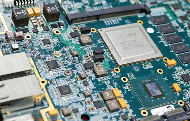
Base stations require PCBs that support massive MIMO antennas, high-frequency RF modules, and power amplifiers in a compact form factor. Traditional PCBs struggle with the routing density needed for fine-pitch BGAs and connectors used in these applications. HDI PCBs enable base station PCB miniaturization by reducing overall board dimensions by integrating more functionality per unit area. This is critical for remote radio heads mounted on towers, where weight and size directly impact installation costs and aerodynamics. Moreover, the shorter interconnect paths in HDI designs minimize signal loss and crosstalk, vital for maintaining data throughput in dense spectrum environments. Reliability under harsh outdoor conditions further underscores their relevance.
Key Benefits of HDI PCBs in Base Stations
One primary advantage of HDI PCBs lies in their support for base station PCB miniaturization, allowing engineers to fit advanced processors and transceivers into smaller enclosures. Microvias PCB technology reduces layer count for equivalent density, leading to thinner profiles and lower material costs over time. High-density interconnect features improve signal integrity by shortening transmission lines, which is essential for high-speed data handling in 5G base stations. Fine-pitch PCB capabilities enable direct connection to components with pitches under 0.8 mm, eliminating the need for larger fanout areas. Thermal performance benefits from closer component spacing and embedded vias for heat dissipation. Overall, these attributes enhance system efficiency and scalability.
Technical Principles Behind High-Density Interconnect
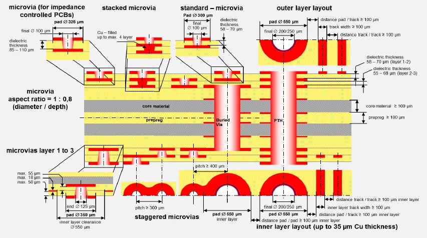
High-density interconnect relies on microvia formation, where laser ablation creates openings as small as 75 microns in dielectric materials. These vias can be blind, buried, staggered, or stacked, each serving specific routing needs in multilayer stackups. Staggered microvias offset between layers to avoid alignment issues, while stacked ones provide direct vertical paths for critical signals. Fine-pitch traces demand precise control of line width and spacing to prevent shorts during fabrication. Material selection focuses on low-loss dielectrics compatible with laser drilling and high-frequency operation. Impedance matching becomes a core principle, as microstrip and stripline geometries must account for the thinner cores typical in HDI designs.
The electrical performance stems from reduced parasitic inductance and capacitance due to smaller via dimensions. Engineers model these effects using field solvers to predict crosstalk in dense fine-pitch PCB layouts. Mechanical reliability involves managing via aspect ratios, typically limited to 1:1 or less, to ensure plating uniformity. Thermal expansion mismatch between copper and resin requires careful stackup planning. These principles collectively enable HDI PCBs to outperform standard boards in complex telecommunication environments.
Design Considerations for HDI PCBs in Base Stations
Designing HDI PCBs for base stations starts with stackup planning, balancing microvia types with layer count and signal requirements. For instance, a 2+n+2 structure suits HDI PCB applications with outer layer microvias for fine-pitch component escape routing. Microvias PCB reliability hinges on fill processes, such as electroplated copper, to withstand thermal cycling in outdoor deployments. Fine-pitch PCB traces necessitate adjusted etch factors and exposure to achieve uniform widths. Signal integrity analysis must verify controlled impedance across high-speed differential pairs routed near microvias. Power distribution layers benefit from embedded planes connected via filled vias, reducing voltage drops.
Fabrication tolerances tighten for HDI, with drill registration critical for stacked vias. Aspect ratio control prevents voids in plating, a common failure mode under vibration. Environmental factors like humidity demand robust surface finishes compatible with assembly. Testing protocols include thermal shock and electrical continuity checks post-lamination. These considerations ensure the board meets operational demands without compromising yield.
Best Practices and Standards Compliance
Adhering to established guidelines streamlines HDI PCB development for base stations. IPC-2226 provides sectional design rules for high-density interconnect features, including microvia sizing and spacing. Engineers should simulate via transitions early to mitigate reflections in fine-pitch routing. Sequential lamination processes build HDI layers incrementally, allowing inspection at each step. Material qualification verifies laser drillability and CTE matching per IPC specifications.
Qualification follows IPC-6012DS for rigid boards with HDI, specifying performance tests like thermal cycle endurance. Class 3 requirements apply for uninterrupted service in base stations. Documentation of design rules aids manufacturability reviews. These practices minimize iterations and enhance first-pass success.
Conclusion
HDI PCBs revolutionize telecommunication base stations by delivering the density, performance, and compactness required for next-generation networks. Benefits like base station PCB miniaturization, superior signal integrity, and integration of fine-pitch components outweigh the added design complexity. Key considerations in microvias PCB and high-density interconnect implementation ensure reliability in demanding environments. By following structured approaches and relevant standards, engineers can leverage HDI technology effectively. As wireless demands grow, HDI PCBs will remain central to advancing base station capabilities.
FAQs
Q1: What makes HDI PCBs ideal for base station PCB miniaturization?
A1: HDI PCBs use microvias and fine-pitch traces to pack more components into smaller areas, reducing overall board size without sacrificing functionality. This supports compact remote radio units in 5G deployments. Shorter signal paths improve efficiency, and layered structures optimize space. Compliance with design rules ensures manufacturability.
Q2: How do microvias in HDI PCBs enhance signal performance?
A2: Microvias provide precise interlayer connections with minimal stubs, lowering inductance and improving high-frequency response in telecommunication applications. They enable dense routing around fine-pitch BGAs. Stacked or staggered configurations suit different integrity needs. Proper sizing per standards prevents failures.
Q3: What are the main design challenges for fine-pitch PCB in base stations?
A3: Fine-pitch PCB requires tight trace spacing and via-in-pad techniques to fan out high-pin-count devices. Impedance control and crosstalk mitigation demand simulation. Material choices affect drill quality for microvias. Thermal management integrates vias for heat paths.
Q4: Why reference IPC standards in HDI PCB design?
A4: IPC standards like IPC-2226 outline rules for high-density interconnect features, ensuring reliability and consistency. They guide microvia rules and stackups for base station applications. Qualification per IPC-6012DS verifies performance. This approach reduces risks in production.
References
IPC-2226A — Sectional Design Standard for High Density Interconnect (HDI) Printed Boards. IPC, 2017
IPC-6012DS — Space and Military Avionics Applications Addendum to IPC-6012D, Qualification and Performance Specification for Rigid Printed Boards. IPC, 2015
IPC-6012D — Qualification and Performance Specification for Rigid Printed Boards. IPC, 2015


