Introduction
High-density interconnect (HDI) PCBs have become foundational to modern electronics. They enable manufacturers to pack more functionality into smaller footprints while delivering superior electrical performance, thermal management, and long-term reliability. Unlike traditional multilayer PCBs that rely primarily on through-hole vias, This HDI PCB guide explores how these advanced features allow designers to meet the rigorous demands of next-generation hardware.
Understanding HDI PCB Technology and Core Benefits
HDI PCBs are classified by build-up structures such as 1+n+1, 2+n+2, or every-layer-interconnect (ELIC). These configurations use laser-drilled microvias, sequential lamination, and via filling (copper or conductive epoxy) to create vertical interconnections without consuming excessive horizontal space. Key enablers include low Dk/Df laminates for high-frequency performance, controlled impedance routing, via-in-pad designs, and symmetric stackups to minimize warpage.
Core benefits across virtually all HDI PCB applications include:
- Miniaturization: Reduced layer count, smaller vias, and denser routing shrink board size and overall product volume — critical for wearables, implants, and remote radio heads.
- Signal Integrity: Shorter interconnects lower parasitic inductance, capacitance, and signal attenuation. They reduce crosstalk and reflections, especially important at gigahertz frequencies.
- Thermal Management: Closer component placement combined with thermal vias, filled microvias, and embedded copper planes improves heat dissipation in high-power RF modules or processing units.
- Reliability: Fewer mechanical drill holes, better aspect ratios (often ≤1:1 for microvias), and robust materials enhance performance under thermal cycling, vibration, humidity, and electromagnetic stress.
- Power Efficiency and EMI Reduction: Optimized power distribution networks and shorter paths support lower power consumption and better electromagnetic compatibility (EMC).
These advantages explain why HDI technology has seen rapid adoption. The global market continues to grow as industries demand smaller, faster, and more reliable electronics.
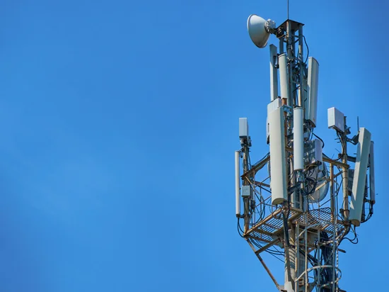
Implementing Advanced HDI Solutions in Telecommunication Base Stations
In modern wireless infrastructure, the role of HDI PCBs in telecommunication base stations is pivotal. Base stations, especially 5G remote radio heads (RRHs) mounted on towers or in dense urban environments, face severe constraints on size, weight, power, and thermal performance. HDI technology addresses these by enabling massive MIMO antenna arrays, high-frequency RF modules, and power amplifiers within compact enclosures.
Key benefits include base station PCB miniaturization (thinner profiles and reduced material costs through fewer layers), superior signal integrity for high-speed data in dense spectrum environments, enhanced thermal management via filled vias and strategic component placement, and improved system scalability for evolving network demands.
Design considerations emphasize meticulous stackup planning (e.g., 2+n+2 configurations), microvia types (blind, buried, staggered, or stacked), fine-pitch trace control, impedance matching for differential pairs, and power integrity through embedded planes. Materials must offer low-loss characteristics and good laser drillability. Fabrication relies on sequential lamination, precise registration, and compliance with standards such as IPC-2226 for HDI design rules and IPC-6012DS Class 3 for high-reliability performance in outdoor conditions.
Challenges involve managing fabrication tolerances, thermal cycling in harsh environments, crosstalk in dense layouts, and balancing cost with yield. For a full exploration of benefits, design rules, and implementation strategies tailored to telecom infrastructure, read our cluster article: The Role of HDI PCBs in Telecommunication Base Stations: Benefits and Design Considerations.
Mastering HDI Layout Techniques for Next-Generation 5G Systems
HDI PCB design for 5G applications demands exceptional control over high-frequency signals (including millimeter-wave bands), low latency, and high bandwidth. 5G base stations, small cells, smartphones, and infrastructure equipment require boards that maintain signal integrity while supporting dense component integration and efficient thermal dissipation.
Critical design strategies include balanced stackups with alternating signal and ground planes, strategic microvia placement to shorten paths and reduce parasitic effects, matched-length differential pairs, smooth trace routing (avoiding sharp angles), and incorporation of thermal vias or heat-spreading layers. Material selection focuses on low dielectric constant (Dk) and dissipation factor (Df) laminates to minimize attenuation and support impedance control.
Benefits for 5G include reduced signal loss and crosstalk, enabling higher data rates; compact form factors for dense urban deployments; and improved power distribution for power-hungry RF and baseband processors. Challenges center on managing signal integrity at elevated frequencies, thermal stress in multilayer builds, crosstalk in dense routing, and the manufacturing precision required for fine features and complex vias.
Best practices involve adherence to IPC-2226, extensive simulation for SI/PI, via-in-pad where appropriate, and symmetrical designs to reduce warpage. Explore these topics in depth in our dedicated cluster page: HDI PCB Design for 5G Applications.

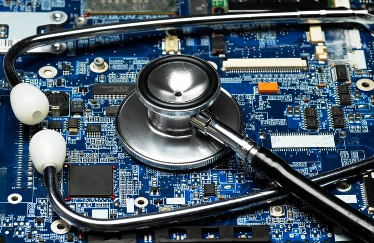
Streamlining Production Processes for HDI PCBs in Miniature Medical Devices
Beyond imaging systems, high-density interconnect PCBs optimizing manufacturing capacity for compact medical devices are essential for wearables, portable diagnostics, implantables, and handheld ultrasound units. These applications require high reliability under sterilization, vibration, thermal cycling, and biological exposure while maintaining strict quality standards.
Optimizing production involves design for manufacturability (DFM) reviews focused on symmetric stackups, via fill completeness, and registration accuracy. Sequential lamination with laser drilling (UV/CO2 for microvias <150 μm in thin dielectrics <50 μm), plasma desmear, copper electroplating, and planarization are standard. Low-CTE resins, uniform drillable materials, ENIG finishes, and filled vias improve yield and reliability. Panelization strategies, automation, statistical process control, in-line inspection (AOI, cross-sectioning), and traceability support scalability — one case study showed doubled throughput for a 12-layer 2-10-2 board used in portable analyzers.
Benefits include smaller device footprints, longer battery life, faster time-to-market, and compliance with medical-grade reliability (IPC-6012DS Class 3, J-STD soldering). Challenges include lower initial yields, longer cycle times from multiple lamination steps, defect propagation in stacked structures, and the need for rigorous qualification. Early fabricator collaboration and standardized processes are critical for cost control and volume scaling.
Read the full manufacturing-focused guide here: High-Density Interconnect PCBs: Optimizing Manufacturing Capacity for Compact Medical Devices.
HDI PCB Applications in Automotive, Aerospace, Consumer Electronics, and IoT
Automotive electronics increasingly rely on HDI for ADAS radar modules, LiDAR, cameras, infotainment, and EV battery management systems. HDI delivers the vibration and temperature resilience, high-frequency routing for radar, and space savings needed in modern vehicles. Thermal stability, reliable microvias, and robust materials help boards survive automotive-grade qualification.
In aerospace and defense, HDI PCBs are chosen for avionics, satellites, missile systems, and communications equipment where weight savings, extreme environment tolerance (shock, vibration, thermal cycling, radiation), and high reliability are non-negotiable. Stacked microvias and high-density designs reduce overall system mass while maintaining performance in hazardous conditions.
Consumer electronics represent the largest volume application. Smartphones routinely use ELIC HDI constructions, while wearables (smartwatches, fitness trackers, VR/AR headsets), tablets, and thin laptops depend on HDI for sleek profiles, high processing power, extended battery life, and dense sensor integration.
IoT devices benefit from HDI through extreme miniaturization of sensor nodes, wireless modules, and gateways. When combined with flexible or rigid-flex constructions, HDI supports foldable enclosures, lower power consumption via reduced signal loss, and higher component counts in battery-powered edge devices.
Across these sectors, common themes emerge: shorter signal paths improve performance, microvia technology enables density, and careful material and stackup choices address thermal and mechanical demands.
Cross-Application Design Considerations and Best Practices
Successful HDI PCB applications share several best practices regardless of industry:
- Early DFM collaboration with fabricators.
- Comprehensive SI/PI/thermal simulation before layout finalization.
- Symmetric stackups and balanced copper distribution to control warpage.
- Strategic via placement (staggered vs. stacked depending on reliability needs).
- Controlled impedance routing with verified low Dk/Df materials.
- Adherence to IPC-2226, IPC-6012DS/6016, and Class 3 reliability where required.
- Via filling, planarization, and robust surface finishes (ENIG, etc.).
These steps reduce iterations, improve yield, and ensure the board meets application-specific stresses.
Challenges and Future Trends in HDI PCB Applications
Common challenges include higher upfront costs, manufacturing complexity (laser precision, registration, yield management), potential reliability issues with stacked microvias under extreme stress, and the need for specialized testing. Thermal hotspots in ultra-dense designs and regulatory hurdles in medical/aerospace applications require careful engineering.
Future trends point toward even finer features, new materials (LCP, advanced low-loss laminates, graphene-enhanced substrates), tighter integration with rigid-flex and embedded component technology, AI-assisted design and simulation, and sustainable manufacturing processes. Applications will expand with 6G, implantable medical electronics, autonomous vehicles, AI edge computing, and advanced IoT ecosystems. As demands for performance and miniaturization grow, HDI will remain at the center of electronics innovation.
Conclusion
HDI PCB applications span telecommunications base stations, 5G infrastructure, high-field MRI systems, portable and implantable medical devices, automotive safety systems, aerospace platforms, consumer gadgets, and IoT networks. By enabling miniaturization without sacrificing signal integrity, thermal performance, or reliability, high-density interconnect technology continues to drive progress across industries.
The refined insights from our cluster pages — covering the role of HDI PCBs in telecommunication base stations, HDI PCB design for 5G applications, advantages and challenges in MRI machines, and manufacturing optimization for compact medical devices — demonstrate both the versatility and the technical rigor required. Partnering with an experienced manufacturer like Aivon ensures designs are optimized for performance, cost, and scalability from prototype through volume production.
FAQs
Q1: What are the most important HDI PCB applications in 2026?
A1: HDI PCBs are heavily used in 5G and telecommunication base stations, MRI and medical imaging equipment, wearable and implantable medical devices, automotive ADAS/radar modules, aerospace avionics, smartphones, and IoT sensor nodes. Their combination of microvias, fine traces, and dense integration makes them ideal wherever size, speed, and reliability are critical.
Q2: What should designers focus on for successful HDI PCB design for 5G applications?
A2: Prioritize symmetrical stackups, low Dk/Df materials, precise impedance control, short microvia paths, thorough SI/PI simulation, thermal via strategies, and early manufacturer collaboration. These elements minimize signal loss, crosstalk, and warpage at millimeter-wave frequencies.
Q3: What are the main differences between HDI PCBs and traditional multilayer boards?
A3: HDI PCBs use laser-drilled microvias (≤150 μm), blind/buried/stacked vias, and finer traces (often <75 μm) instead of primarily mechanical through-hole vias. This enables greater routing density, shorter signal paths, reduced layer counts for equivalent functionality, better signal integrity, and superior miniaturization. Traditional multilayer boards are simpler and cheaper for low-density designs but cannot match HDI performance in 5G, medical, or high-reliability HDI PCB applications.


