Introduction
Internet of Things (IoT) devices continue to evolve with smaller form factors and higher component densities, pushing printed circuit boards (PCBs) to their thermal limits. High-density designs pack processors, sensors, and power management ICs into compact spaces, where heat generation from power dissipation becomes a critical concern. Overheating can lead to reduced component lifespan, signal integrity issues, and outright system failures, making effective thermal management essential for reliable operation. Engineers must address these challenges early in the design phase to ensure IoT devices perform consistently in diverse environments, from smart homes to industrial sensors. This article explores proven strategies for thermal vias PCB design, heat sink PCB integration, thermal simulation PCB processes, high power PCB cooling, and PCB thermal analysis techniques tailored to high-density IoT applications.
Why Thermal Management Matters in High-Density IoT PCBs
High-density IoT PCBs face intensified thermal stresses due to closely spaced components and limited airflow paths. Power-hungry elements like microcontrollers and wireless modules generate localized hotspots that propagate through the board, elevating junction temperatures beyond safe limits. Without proper management, these hotspots cause electromigration in traces, delamination in laminates, and premature aging of solder joints. Industry standards such as IPC-2221 provide foundational guidelines for designing boards that maintain thermal stability under load. Effective thermal management not only extends device reliability but also optimizes performance by preventing throttling in processors. For electric engineers, prioritizing PCB thermal analysis from the outset minimizes costly redesigns and field failures.
Fundamental Principles of Heat Transfer in PCBs
Heat in PCBs transfers primarily through conduction, convection, and radiation, each playing a role depending on the design and environment. Conduction dominates within the board, where copper layers and vias act as pathways to spread heat from sources to sinks. Convection occurs at surfaces exposed to air or forced flow, while radiation contributes minimally in typical IoT enclosures. Material properties like thermal conductivity of copper (around 400 W/mK) versus FR-4 (0.3 W/mK) dictate efficient paths. Engineers must balance these mechanisms by optimizing stackups with inner planes for horizontal spreading and vias for vertical conduction. Understanding these principles forms the basis for implementing thermal vias PCB design and other solutions.
Role of Thermal Vias in PCB Design
Thermal vias PCB design involves placing arrays of plated through-holes under or near heat-generating components to channel heat vertically through the board stackup. These vias connect surface pads to inner copper planes, creating low-impedance thermal paths that bypass the low-conductivity laminate. In high-density IoT boards, via-in-pad techniques place vias directly beneath exposed pads of power ICs, maximizing contact area. Arrays typically feature small diameters for density, with pitches ensuring manufacturability and avoiding solder wicking during assembly. Filled thermal vias, plugged with conductive epoxy, enhance reliability by reducing voids and improving mechanical strength. Proper placement prevents hotspots from concentrating under components, distributing heat evenly across layers.
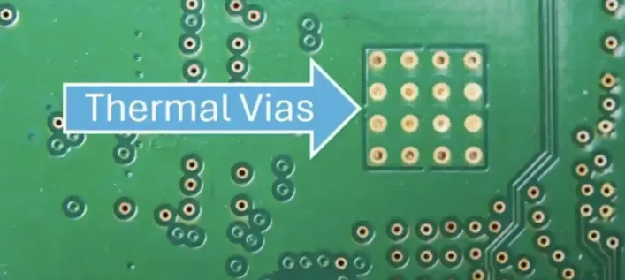
Engineers should cluster 10 to 20 vias per square millimeter under high-power devices, adjusting based on power levels. This approach aligns with best practices for multilayer boards, where multiple via layers bridge planes effectively. Avoiding excessive via density prevents drill breakout and plating issues during fabrication. Thermal vias prove indispensable in IoT designs with fine-pitch BGAs, where surface area for cooling is scarce.
Integrating Heat Sinks into PCB Designs
Heat sink PCB integration requires careful mechanical and thermal interfacing to maximize dissipation without compromising board integrity. Surface-mount heat sinks attach via thermal interface materials (TIMs) like pads or pastes, filling microscopic air gaps for optimal conduction. For high-density IoT PCBs, low-profile pin-fin or stamped designs fit within enclosures while promoting natural convection. Mechanical clips or epoxy bonding secure sinks to components, distributing stress evenly to avoid board warpage. In double-sided assemblies, underside heat sinks demand via stitching to couple heat from top to bottom layers. This integration lowers component temperatures significantly, especially in battery-powered devices sensitive to thermal runaway.
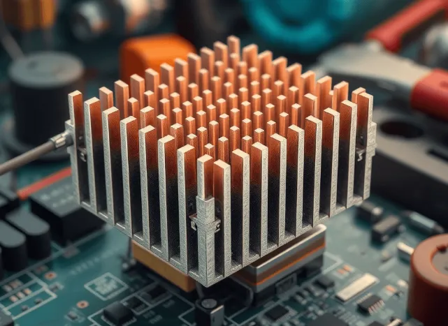
Selection criteria include fin spacing for airflow and base flatness for contact efficiency. Engineers often combine heat sinks with copper pours extending from component lands, forming hybrid spreaders. Vibration-prone IoT applications benefit from epoxy over clips for stability. Overall, heat sink PCB integration complements internal strategies, providing boundary cooling for sustained operation.
Leveraging Thermal Simulation and PCB Thermal Analysis
Thermal simulation PCB tools model heat flow using finite element analysis (FEA) or computational fluid dynamics (CFD), predicting temperatures across the board under real-world loads. Engineers input power dissipation, material properties, and boundary conditions to visualize hotspots and gradients. PCB thermal analysis reveals via effectiveness, plane contributions, and sink performance before prototyping. Iterative simulations refine stackups, such as adding dedicated thermal layers between signal planes. Validation against standards like IPC-2152 ensures trace widths support current without excessive rise. This upfront analysis cuts development time and prevents thermal bottlenecks in high-density designs.
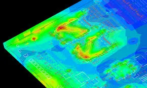
Mesh refinement focuses on critical areas like via farms and ICs for accuracy. Coupled electro-thermal models account for resistance changes with temperature. Post-simulation, engineers correlate predictions with infrared thermography on prototypes. Comprehensive PCB thermal analysis integrates seamlessly into the design flow, enabling data-driven decisions.
High Power PCB Cooling Strategies for IoT
High power PCB cooling in IoT demands multilayer strategies beyond basic vias and sinks. Thick copper layers (2 oz or more) on outer and inner planes spread heat horizontally, while embedded copper coins under hotspots provide direct conduction paths. Metal-core boards, with aluminum substrates, excel in LED drivers or power converters common in IoT gateways. Via tents and stitching connect components to chassis grounds acting as heat sinks. Passive techniques suffice for most edge devices, reserving active fans for gateways with sustained loads. These methods maintain junction temperatures below 125°C, preserving reliability.
Hybrid approaches layer conduction-dominant internals with convection-focused externals. Engineers prioritize plane symmetry to avoid thermal bowing. For ultra-high density, microchannel cold plates integrate directly, though costlier. High power PCB cooling evolves with IoT power trends, balancing efficiency and size.
Best Practices for Implementation
Start with stackup planning, allocating inner layers for power and ground planes adjacent to signal layers for coupling. Place high-power components centrally or near board edges for sink access, minimizing trace lengths. Incorporate thermal relief pads on vias to ease soldering while preserving conduction. During layout, route wide traces per IPC-2152 for current capacity, integrating them into pours. Prototype testing with thermocouples validates simulations, iterating on via counts or TIM thickness. Documentation of thermal budgets ensures supply chain alignment.
Quick reference:
- Thermal Vias — Application: Under ICs; Key Benefit: Vertical heat transfer
- Copper Planes — Application: Full layers; Key Benefit: Horizontal spreading
- Heat Sinks — Application: Exposed components; Key Benefit: Surface convection
- Filled Vias — Application: High-reliability; Key Benefit: Void prevention
Adhering to these practices yields robust IoT PCBs resilient to thermal extremes.
Troubleshooting Thermal Issues in High-Density Designs
Hotspots persisting post-simulation often stem from underestimated power or poor via placement. Inspect for delamination via X-ray, addressing with bake-out per JEDEC guidelines. Warpage from asymmetric heating requires balanced copper distribution. Assembly defects like insufficient TIM manifest as elevated resistances; reworking with fresh material resolves them. Field failures trace to enclosure airflow restrictions, necessitating vents or ducts. Systematic PCB thermal analysis pinpoints root causes, guiding fixes efficiently.
Conclusion
Mastering IoT PCB thermal management hinges on integrated strategies like thermal vias PCB design, heat sink PCB integration, and rigorous thermal simulation PCB workflows. High-density designs demand proactive high power PCB cooling and PCB thermal analysis to avert overheating pitfalls. By applying these engineering principles and standards, designers achieve reliable, efficient devices. Prioritizing thermal integrity from concept to production ensures IoT systems thrive in demanding applications. Electric engineers equipped with these tools can innovate confidently, delivering performance without compromise.
FAQs
Q1: What role do thermal vias play in PCB design for IoT devices?
A1: Thermal vias in PCB design create vertical conduction paths from surface components to inner planes, crucial for high-density IoT boards. Arrays under power ICs distribute heat, preventing localized hotspots. Proper sizing and filling enhance reliability, aligning with manufacturing tolerances. This technique supports compact layouts without external cooling.
Q2: How does heat sink PCB integration improve high power cooling?
A2: Heat sink PCB integration uses TIMs and mechanical fasteners to couple sinks directly to components, boosting convection dissipation. In high power PCB cooling, low-profile designs fit IoT enclosures while lowering temperatures by 20-50°C typically. Placement near edges maximizes airflow. Combined with internal vias, it forms comprehensive thermal paths.
Q3: Why is thermal simulation essential for PCB thermal analysis?
A3: Thermal simulation in PCB thermal analysis predicts heat flow, identifying risks before fabrication. Engineers model stackups and loads to optimize vias and planes. It reduces prototypes and ensures compliance with thermal limits. For high-density IoT, it reveals interactions missed in hand calculations.
Q4: What are common best practices for preventing overheating in high-density PCBs?
A4: Best practices include wide copper pours, symmetric stackups, and thermal vias PCB design under hotspots. Incorporate planes for spreading and sinks for boundary cooling. Perform PCB thermal analysis iteratively. These steps maintain reliability in power-dense IoT applications.
References
IPC-2221B — Generic Standard on Printed Board Design. IPC, 2012
IPC-2152A — Standard for Determining Current Versus Temperature Rise in Printed Board Traces. IPC, 2009
IPC-6012E — Qualification and Performance Specification for Rigid Printed Boards. IPC, 2017


