Introduction
E-readers have transformed from simple digital book displays into sophisticated devices that connect seamlessly with the broader Internet of Things (IoT) ecosystem. Integrating wireless connectivity such as Bluetooth and Wi-Fi into e-reader printed circuit boards (PCBs) allows for real-time content updates, user data synchronization, and interaction with other smart devices. PCB designers must address unique challenges like compact form factors, low power consumption, and reliable signal integrity to make this possible. This article explores the engineering principles behind e-reader PCB design optimized for IoT, focusing on antenna design and wireless protocols. By following structured approaches, engineers can ensure robust performance in battery-powered environments. The result is enhanced functionality that meets the demands of modern connected reading experiences.
The Role of IoT in E-Reader Evolution
IoT integration elevates e-readers beyond standalone devices, enabling features like over-the-air firmware updates and cloud-based library access. Wireless connectivity via Bluetooth and Wi-Fi provides the backbone for these capabilities, allowing e-readers to communicate with smartphones, routers, and cloud servers efficiently. For electric engineers, understanding this shift means prioritizing PCB layouts that support multiple radio frequencies while minimizing interference. Compact e-reader designs often constrain space, making integrated antenna solutions essential for maintaining slim profiles without external modules. Industry relevance grows as consumers expect seamless interoperability in smart homes and personal ecosystems. Proper PCB design ensures compliance with performance standards, reducing failure rates in real-world deployments.
E-readers operate in low-power states for extended battery life, so IoT features must activate only when needed. Bluetooth Low Energy (BLE) suits intermittent data transfers like syncing reading progress, while Wi-Fi handles larger downloads such as book files. Engineers must balance these protocols on shared PCB real estate, avoiding crosstalk between 2.4 GHz bands. Antenna design plays a pivotal role here, as poor implementation leads to reduced range and data throughput. As IoT adoption surges, e-reader PCBs that enable reliable wireless connectivity become a competitive edge for device longevity and user satisfaction.
Fundamental Principles of Wireless Connectivity in E-Reader PCBs
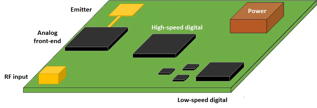
Wireless connectivity in e-readers relies on precise RF signal paths from the chipset to the antenna, demanding careful PCB stackup and trace routing. Multi-layer boards typically feature dedicated RF layers with controlled impedance, usually 50 ohms for both Bluetooth and Wi-Fi signals. Ground planes act as shields, preventing noise coupling from digital circuits like the display driver or processor. Engineers calculate trace widths using dielectric constants of the substrate, ensuring minimal insertion loss at 2.4 GHz. Vias must be back-drilled or staggered to avoid stubs that reflect signals and degrade performance. These principles form the core of antenna design, where radiation patterns determine coverage in handheld orientations.
Antenna types for e-reader PCBs include inverted-F antennas (IFAs) and planar inverted-F antennas (PIFAs), favored for their compact size and omnidirectional patterns. These structures require clearance areas free of metal, often 10-15% of the PCB surface, to avoid detuning. Matching networks with pi-filters or L-C components tune the antenna to the chipset's output impedance, maximizing power transfer. Simulations verify standing wave ratio (SWR) below 2:1 across operating bands. Bluetooth demands lower power handling than Wi-Fi, so shared antennas use switches to isolate paths. Ground plane size directly influences bandwidth, with larger planes enhancing efficiency in e-readers' typical 100-200 mm dimensions.
Power management integrates tightly with wireless sections, as IoT protocols draw significant current during transmission. Low-dropout regulators and DC-DC converters supply clean power to RF front-ends, with decoupling capacitors placed within 1 mm of pins. Sleep modes deactivate radios, preserving battery life critical for weeks-long usage. Thermal considerations arise from Wi-Fi bursts, requiring vias for heat dissipation to nearby grounds. Electromagnetic compatibility (EMC) testing ensures emissions stay within limits, preventing interference with the e-ink display's refresh cycles. IPC-6012E provides qualification guidelines for rigid PCBs in such high-reliability applications.
Signal integrity challenges intensify with IoT's data demands, where Bluetooth handles short packets and Wi-Fi streams larger payloads. PCB materials with low loss tangents, like FR-4 variants optimized for RF, reduce attenuation. Coplanar waveguide (CPW) structures offer better shielding than microstrips in dense layouts. Antenna placement near edges maximizes ground coupling, improving gain by 2-3 dBi. Multipath fading in indoor environments necessitates diversity antennas, though space limits this to single-element designs. Engineers iterate layouts using field solvers to predict real-world behavior before fabrication.
Best Practices for PCB Design in IoT-Enabled E-Readers
Start with schematic capture emphasizing modular RF sections, isolating digital and analog grounds with stitching vias. Route Bluetooth and Wi-Fi traces first, maintaining lengths under lambda/20 at 2.4 GHz to minimize phase shifts. Antenna design prioritizes symmetry, avoiding bends sharper than 45 degrees that introduce discontinuities. Place Wi-Fi module baluns near the antenna feed to suppress common-mode currents. For Bluetooth, co-location with the processor reduces trace lengths, aiding low-energy efficiency. Verify designs against JEDEC J-STD-020E for component reflow sensitivity, as wireless ICs often classify at MSL 3.
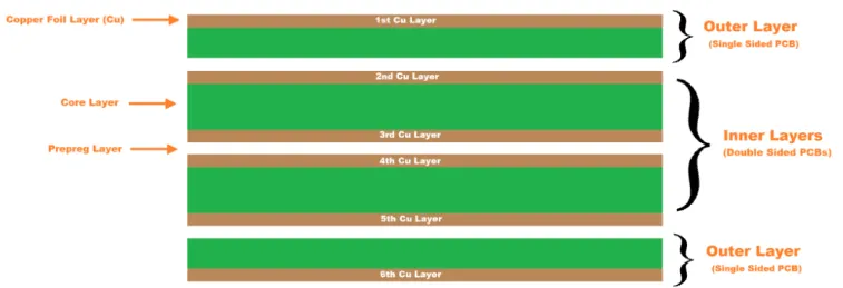
Layer stackup defines success: signal-ground-signal for RF, with power planes segmented. Core thickness around 0.8 mm supports thin profiles while providing mechanical stability. Solder mask cutouts over antennas prevent dielectric loading, preserving resonance. Testing involves vector network analyzers for return loss and radiated patterns in anechoic chambers. Firmware calibration adjusts for manufacturing tolerances in antenna tuning. These practices ensure wireless connectivity reliability across production volumes.
Shielding cans enclose noisy sections, grounded at multiple points to contain EMI. Ferrite beads on power lines filter high-frequency noise from switching regulators. For dual-band operation, notch filters reject harmonics. Assembly follows IPC-A-600K acceptability criteria, inspecting solder joints under RF paths for voids. Field strength measurements confirm minimum viable signal levels for IoT handshakes. Engineers document deviations, enabling yield improvements in iterations.
Component selection favors integrated SoCs combining Bluetooth and Wi-Fi, reducing PCB footprint. Passives rated for RF voltages prevent arcing in high-power Wi-Fi modes. Board-level shielding via ground pours around crystals stabilizes clock references. Environmental robustness includes conformal coatings for humidity resistance in portable use. Prototyping with flex-rigid hybrids accommodates curved e-reader forms. Comprehensive design reviews catch issues like inadequate via fencing early.
Common Challenges and Engineering Solutions
Integration density causes crosstalk between Bluetooth and Wi-Fi, mitigated by frequency-selective shielding and orthogonal polarizations. Battery voltage droop during transmits triggers resets, solved with hold-up capacitors sized for peak currents. Antenna detuning from chassis metal requires parasitic elements for compensation. Yield losses from warpage affect fine-pitch RF BGAs, addressed by bake-out per JEDEC guidelines before reflow. Debugging uses spectrum analyzers to isolate spurs from LCD drivers. Solutions emphasize simulation-driven design, cutting physical spins.
Overheating in prolonged Wi-Fi sessions demands thermal vias and cutouts. Software-defined power profiles adapt to link quality, conserving energy. Multi-protocol stacking on shared hardware needs robust coexistence mechanisms like time-division multiplexing. Mechanical stress from flexing affects trace integrity, so strain-relief anchors secure connections. Post-assembly tuning with laser-trimmed networks fine-tunes matching. These targeted fixes elevate IoT performance in constrained e-reader PCBs.
Conclusion
E-reader PCB design for IoT integration hinges on masterful antenna design and wireless connectivity optimization for Bluetooth and Wi-Fi. Engineers achieve this through precise impedance control, shielding, and power management, ensuring low-power, reliable operation. Adhering to standards like IPC-6012E guarantees quality in production. These principles enable e-readers to thrive in connected ecosystems, delivering uninterrupted user experiences. Future designs will push boundaries with 5G and ultra-wideband, but fundamentals remain unchanged. Prioritizing structured engineering yields robust, future-proof solutions.
FAQs
Q1: What antenna design considerations are critical for IoT wireless connectivity in e-readers?
A1: Antenna design must prioritize compact inverted-F structures with 50-ohm matching networks to support Bluetooth and Wi-Fi at 2.4 GHz. Clearance zones and ground plane sizing ensure efficient radiation patterns, avoiding detuning from nearby components. Engineers simulate SWR and gain to meet range requirements in handheld use. Proper integration minimizes losses, enabling seamless IoT data exchange without external antennas.
Q2: How does PCB layout impact Bluetooth and Wi-Fi performance in e-reader IoT applications?
A2: Layout routing keeps RF traces short and shielded, with ground vias preventing crosstalk between Bluetooth and Wi-Fi paths. Multi-layer stackups isolate signals from digital noise, maintaining signal integrity. Decoupling near ICs stabilizes power, crucial for low-energy protocols. Following these practices boosts throughput and reduces packet errors in compact designs.
Q3: Why is power management essential for wireless connectivity on e-reader PCBs?
A3: Power management prevents voltage drops during Wi-Fi transmits, using regulators and capacitors to sustain RF performance. Sleep modes deactivate radios, extending battery life vital for IoT features like syncing. Thermal vias dissipate heat from bursts, ensuring reliability. Optimized designs balance connectivity demands with portable constraints.
Q4: What role do industry standards play in e-reader PCB design for IoT?
A4: Standards like IPC-6012E qualify rigid boards for high-reliability wireless applications, specifying material and fabrication tolerances. JEDEC J-STD-020E guides component handling to avoid reflow damage in RF sections. These ensure consistent quality, reducing field failures in Bluetooth and Wi-Fi enabled devices.
References
IPC-6012E — Qualification and Performance Specification for Rigid Printed Boards. IPC, 2017
IPC-A-600K — Acceptability of Printed Boards. IPC, 2020
JEDEC J-STD-020E — Moisture/Reflow Sensitivity Classification. JEDEC, 2014


