Typical Specification Range
| Parameter | Standard parameters for 2 layer aluminum core PCBs |
|---|---|
| Layer count | 2 layers |
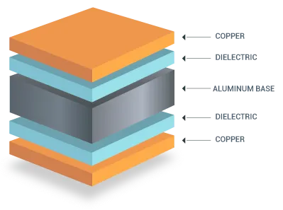
| Material type | Aluminum substrate with thermal dielectric |
| Surface finish | ENIG, HASL, OSP |
| Thickness | 0.8mm to 2.5mm |
| Solder mask | White, green, black |
| Copper thickness | 1oz to 2oz |
| Special features | Thermal vias, aluminum base heat sinking, controlled lamination |
Manufacturing Process Insights
Lamination bonds dielectric film and copper foil to both sides of the aluminum core under controlled pressure.
Drilling requires specialized parameters and tools to limit burr formation on aluminum edges.
Plating involves aluminum surface pretreatment to ensure reliable copper adhesion in through holes.
Surface finish selection balances solderability, cost, and operating environment needs.
Process controls focus on thermal management during lamination and drilling to prevent delamination and maintain via integrity.
Manufacturing Order Profile
| Order Quantity | Order Proportion | Estimated Price Level | Typical Lead Time |
|---|---|---|---|
| Prototype (<=30 pcs) | 67% | From $109 | From 8 days |
| Small volume (30-200 pcs) | 17% | From $137 | From 10 days |
| Mass production (>200 pcs) | 16% | From $224 | From 11 days |
Manufacturing Challenges & Process Optimization
Design Considerations
Related Products
Common Applications
PCB Solution for LED Lighting
Maximize LED performance with our specialized metal-core PCBs (MCPCBs), engineered for superior thermal management in high-power lighting systems. We ensure extended lifespans for commercial applications, while our versatile flexible PCBs enable innovative, complex geometries. Achieve peak efficiency and design freedom with our advanced solutions.
PCB Solution for Automotive Electronics
AIVON automotive electronics PCBs are designed for demanding vehicle environments. They withstand extreme temperatures, vibration, and harsh conditions, supporting ECUs, ADAS, infotainment, and EV modules. Featuring multilayer, rigid-flex, and high-frequency designs, AIVON PCBs meet IATF 16949 standards for safe and reliable automotive performance.
PCB Solution for Power Supply
Maximize power density and safety with AIVON’s specialized power supply PCBs. Engineered to handle high currents and thermal loads, our designs feature thick copper, thermal vias, and strict high-voltage isolation. We ensure superior efficiency and robust stability for applications ranging from chargers to industrial converters.
Real Production Records
| Order ID | PCB Type | Layers | Dimensions | Solder Mask | Surface Finish | Quantity | Action |
|---|---|---|---|---|---|---|---|
| Loading... | |||||||
View More Engineering Resources
Why Choose AIVON for 2 Layer Aluminum PCB?
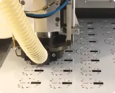
With our own advanced production facility, AIVON manufactures 2 Layer Aluminum PCBs using premium aluminum substrate and precise thermal dielectric control to achieve excellent heat dissipation. In-house lamination, drilling, and copper plating processes ensure tight dimensional tolerances and reliable performance for LED lighting and power applications.
Aluminum PCB Manufacturing Process
Discover the complete aluminum PCB manufacturing process—from material selection and lamination to etching, drilling, and surface finishing. Ideal for high-frequency and prototype applications. Learn technical principles, design requirements, and real-world challenges with expert solutions.
Read More
Design Considerations for Aluminum PCBs in Power Electronics
Aluminum PCB design rules guide power electronics projects for optimal thermal and electrical performance. Learn current capacity calculations, high voltage handling, creepage and clearance distances, plus isolation requirements. Practical tips ensure reliability in inverters, converters, and high power systems. (198 characters)
Read More


