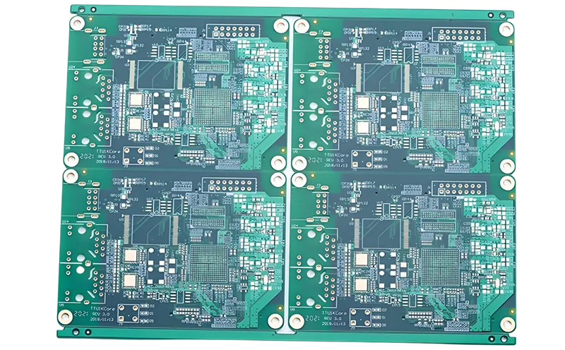
Typical Specification Range
| Parameter | HDI configurations with OSP surface finish |
|---|---|
| Layer count | 4-18 layers |
| Material type | High Tg FR-4, low CTE materials |
| Surface finish | OSP |
| Thickness | 0.8-2.5 mm |
| Solder mask | Photoimageable solder mask |
| Copper thickness | 0.5-2 oz |
| Special features | Microvias, blind vias, stacked vias, fine lines |
Manufacturing Process Insights
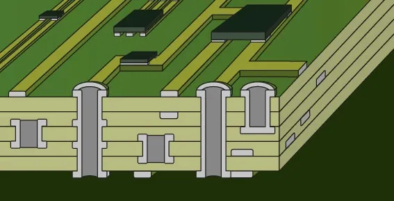
Lamination
Sequential lamination builds HDI layers with tight registration control between cores and prepregs.
Drilling and Plating
Laser drilling forms microvias. Plasma desmear prepares hole walls before direct copper plating.
Surface Finish Logic
OSP is applied post solder mask on exposed copper. Microetch prepares uniform surface for organic coating.
Risk Control
Monitor copper topography and bath chemistry. This prevents oxidation and ensures consistent solderability across dense HDI features.
Manufacturing Order Profile
| Order Quantity | Order Proportion | Estimated Price Level | Typical Lead Time |
|---|---|---|---|
| Prototype (<=30 pcs) | 39% | From $185 | From 8 days |
| Small volume (30-200 pcs) | 41% | From $216 | From 8 days |
| Mass production (>200 pcs) | 20% | From $329 | From 8 days |
Manufacturing Challenges & Process Optimization
Design Considerations
Related Products
Common Applications
PCB Solution for Consumer Electronics
AIVON's consumer electronics PCBs are precision-engineered for smartphones, tablets, laptops, and smart home devices. Using HDI design, fine-line etching, and multilayer fabrication, they deliver compact layouts, high-speed signal transmission, and strong reliability while meeting international quality and environmental standards.
PCB Solution for Industrial Control
AIVON engineers rugged PCBs for industrial control systems demanding unwavering reliability in harsh environments. Featuring high-Tg materials, heavy copper, and conformal coatings, our solutions withstand extreme heat and vibration. We ensure superior signal integrity and long-term stability for PLCs, robotics, and drives, maximizing your operational uptime.
PCB Solution for Telecommunication
AIVON telecommunication PCBs are high-performance boards designed for fast and stable signal transmission. Used in base stations, routers, satellite systems, and 5G infrastructure, they feature advanced materials and precision manufacturing to ensure low signal loss, accurate impedance control, and reliable high-frequency performance.
Real Production Records
| Order ID | PCB Type | Layers | Dimensions | Solder Mask | Surface Finish | Quantity | Action |
|---|---|---|---|---|---|---|---|
| Loading... | |||||||
View More Engineering Resources
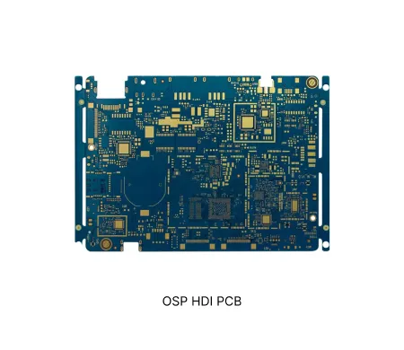
Why Choose AIVON for OSP HDI PCB?
As a vertically integrated factory, AIVON produces OSP HDI PCBs with advanced laser drilling for microvias and precise OSP coating for superior flatness and solderability. Our in-house multilayer lamination, precise registration control, and reliable copper plating deliver tight impedance tolerance and excellent reliability for high-density fine-pitch designs.
The Essential Role of Blind Vias in HDI PCBs
Learn how PCB blind vias enhance HDI PCB design by optimizing space and improving signal integrity. This guide covers their benefits, challenges, and best practices for electrical engineers crafting high performance electronics.
Read More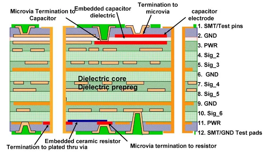
HDI PCB Materials Selection for High Frequency Applications
Learn how to choose HDI PCB materials for high frequency applications. Understand dielectric properties, thermal stability, and industry standards to ensure signal integrity and performance in your next HDI project.
Read More


