Founded in 2013, AIVON is a professional PCB manufacturer dedicated to delivering high-quality printed circuit boards and reliable electronic manufacturing solutions.
Thank you very much for your valuable suggestion!
We will solve it as soon as possible!
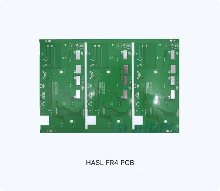
HASL FR4 PCB Manufacturing Insights
Discover how AIVON manufactures HASL FR4 PCBs, including hot air solder leveling processes, surface finish control, fabrication processes, manufacturing challenges, and real production experience from customer orders.
Through-hole compatibility and economical processing
Manufacturing Process Insights
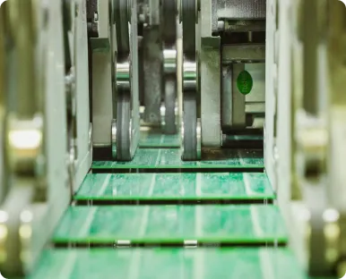
Material Preparation & Lamination FR4 cores are laminated with copper foil under controlled heat and pressure. Symmetric construction helps the board withstand the subsequent thermal shock of the HASL process without excessive warpage.
Drilling & Desmear Through-holes are drilled and chemically cleaned. Clean hole walls are essential so that later solder leveling does not trap residues or create voids inside the barrels.
Pattern Imaging, Plating & Etching Circuits are defined and etched. Adequate annular rings and copper clearances are maintained so that the final HASL coating can form continuous, reliable solderable surfaces.
Solder Mask Application Liquid photoimageable solder mask is applied and developed with precise registration. Via tenting versus open-window decisions are finalized at this stage—critical because open vias will later receive molten solder during HASL.
Hot Air Solder Leveling (HASL) The board is immersed in molten solder (lead-free SnAgCu or traditional SnPb) and leveled by hot-air knives. The process deposits a solder coating on all exposed copper, providing excellent solderability and a relatively low-cost finish. Surface flatness is inherently less uniform than ENIG or OSP.
Silkscreen & Final Forming Legend is printed after HASL. Mechanical routing or V-scoring separates the boards. Final inspection checks for solder bridging, uneven coverage, exposed copper and via condition before shipment.
Manufacturing Order Profile
Order Quantity
Order Proportion
Estimated Price Level
Typical Lead Time
Prototype (<=30 pcs)
45%
From $1
From 1 Day
Small volume (30-200 pcs)
35%
From $30
From 1 Day
Mass production (>200 pcs)
20%
From $50
From 1 Day
Manufacturing Challenges & Process Optimization
Tented Via vs Open Via Conflicts under HASL Order notes and Gerber data frequently disagree on via treatment. Open vias allow molten solder to wick into the barrels during HASL, creating trapped solder beads, contamination or bridging. Tented vias prevent wicking but block probe or soldering access if the design intended open holes. Mixed treatment produces inconsistent results across the panel.
✓ Confirm exact via treatment (full tenting, selective tenting or fully open) before solder-mask generation. ✓ Regenerate mask layers so that open vias retain clear windows and tented vias receive complete coverage. ✓ Prefer tenting for most signal vias when HASL is specified, unless functional access is explicitly required.
View Exact Order Case
Solder Mask Openings & HASL Coverage Control Missing, incomplete or oversized solder-mask openings leave copper either covered by residual ink or excessively exposed. During HASL the exposed copper receives solder while residual mask areas remain non-wettable, producing uneven coating, poor solderability or oxidation sites after the thermal process.
✓ Verify every pad and required via has a correctly sized, clean mask opening. ✓ Avoid residual mask on solderable surfaces and oversized openings that expose non-functional copper. ✓ Cross-check mask expansion against the final HASL process capability.
View Exact Order Case
Edge Copper Exposure after Routing / V-Cut Pads or traces placed too close to the board outline become exposed after contour routing or V-scoring. The subsequent HASL process cannot reliably coat or protect these edge copper features; oxidation, undercut and dendritic growth risk increase, especially on Class 2/3 boards.
✓ Maintain ≥0.3–0.5 mm copper-to-outline clearance on all layers. ✓ Adjust routing compensation and V-cut clearance to prevent copper rollover or exposure. ✓ Inspect edges after HASL for residual exposed copper and cleanliness.
View Exact Order Case
Solder Bridging & Fine-Feature Risks on HASL Surfaces Tight pad-to-pad or pad-to-trace spacing combined with the relatively thick, non-planar HASL coating increases the chance of solder bridges during assembly. Open vias or incomplete mask dams further allow solder to flow uncontrolled during the leveling process itself.
✓ Ensure sufficient spacing for reliable solder-mask bridges after process compensation. ✓ Convert critical dense areas to solder-mask-defined pads when clearance is marginal. ✓ Confirm that via treatment and mask design minimize uncontrolled solder flow under HASL.
View Exact Order Case
Thermal Stress & Via Reliability during HASL The rapid thermal excursion of the HASL process stresses plated through-holes and thin boards. Open vias with residual mask ink or incomplete plating can trap solder beads that later cause intermittent connections or cracking under thermal cycling.
✓ Prefer full tenting or proper plugging for vias that do not require open access. ✓ Ensure clean hole walls and adequate plating thickness before HASL. ✓ For thin boards, verify stackup symmetry so the HASL thermal shock does not induce excessive warpage.
View Exact Order Case
Design Considerations
Via Treatment Strategy for HASL
Decide early whether vias should be tented or left open. Document the choice clearly in both fabrication notes and solder-mask Gerber data. For most signal vias on HASL boards, full tenting is preferred to prevent solder wicking and bead entrapment. Reserve open vias only when probe access or through-hole soldering is required.
Solder Mask Openings & Coverage
Provide complete, correctly sized openings on every solderable pad. Avoid residual mask on copper that must receive HASL and avoid oversized openings that expose non-functional copper. Treat via mask windows as a critical design attribute that must match the chosen via treatment.
Edge Clearance & Outline Integrity
Keep all copper features ≥0.3–0.5 mm from the final board outline. Account for routing and V-cut tolerances so that no copper becomes exposed after depanelization—exposed edge copper is particularly vulnerable after the HASL thermal process.
Spacing Rules for HASL Surfaces
Design pad and trace spacing with the thicker, less planar HASL coating in mind. Maintain adequate clearance for reliable solder-mask bridges. In dense areas, consider solder-mask-defined pads to control final pad geometry and reduce bridging risk during assembly.
Thermal & Mechanical Robustness
Recognize that HASL imposes a significant thermal shock. Use symmetric stackups on thin boards, ensure robust via plating, and avoid open vias that can trap solder. Confirm that silkscreen placement remains legible and adherent after the HASL process.
Maximize power density and safety with AIVON’s specialized power supply PCBs. Engineered to handle high currents and thermal loads, our designs feature thick copper, thermal vias, and strict high-voltage isolation. We ensure superior efficiency and robust stability for applications ranging from chargers to industrial converters.
AIVON's consumer electronics PCBs are precision-engineered for smartphones, tablets, laptops, and smart home devices. Using HDI design, fine-line etching, and multilayer fabrication, they deliver compact layouts, high-speed signal transmission, and strong reliability while meeting international quality and environmental standards.
AIVON engineers rugged PCBs for industrial control systems demanding unwavering reliability in harsh environments. Featuring high-Tg materials, heavy copper, and conformal coatings, our solutions withstand extreme heat and vibration. We ensure superior signal integrity and long-term stability for PLCs, robotics, and drives, maximizing your operational uptime.
View More Engineering Resources
Why Choose AIVON for HASL FR4 PCB?
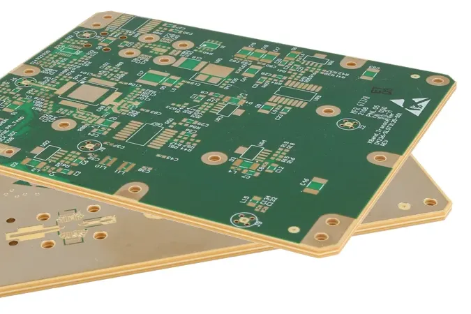
AIVON produces HASL FR4 PCBs with uniform hot air solder leveling for consistent solderability and flat pad surfaces. Precise FR4 material selection, controlled etching, and reliable through-hole plating ensure tight trace tolerances, excellent thermal stability, and long-term solder joint reliability in standard and lead-free HASL finishes.
Quote FR4 PCB Now
The Complete Guide to FR-4 Material Finishes for Optimal Performance
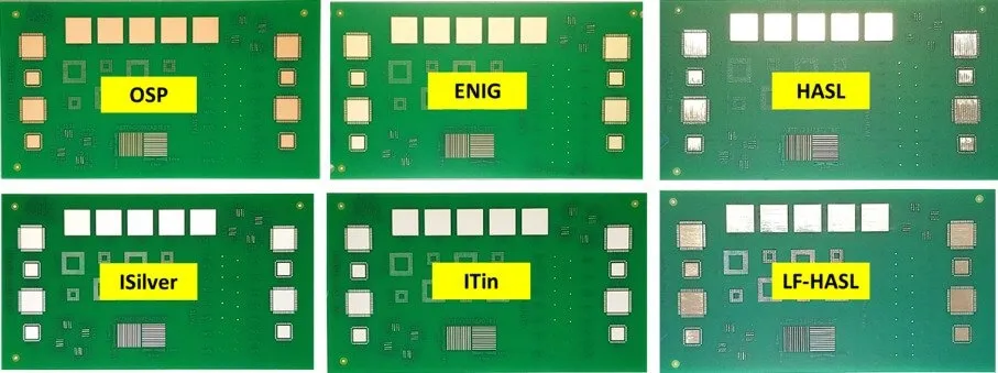
Discover PCB surface finish types like HASL, ENIG, immersion silver, OSP, and ENEPIG: Optimize for solderability, corrosion protection, and reliability on FR-4 boards. Achieve 99% yields with IPC-4552 standards—essential for 2025 high-density assembly.
Exploring Different Finishes for FR 4 PCBs: HASL, ENIG, and More
Compare HASL vs ENIG and other FR-4 PCB surface finishes including immersion silver and OSP. Learn solderability, cost, shelf life, and reliability differences to select the best option for your next project. Lead-free compliant and IPC-standard compliant.