Typical Specification Range
| Parameter | Typical Range |
|---|---|
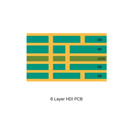
| Layer count | 6 layers |
| Material type | High Tg FR-4, low Dk laminates |
| Surface finish | ENIG, Immersion Silver, OSP |
| Thickness | 0.8mm to 3.0mm |
| Solder mask | Green, black, red, white, yellow, blue, purple, matte black, matte black |
| Copper thickness | 0.5oz to 2oz |
| Special features | Blind and buried vias, stacked microvias, impedance control, Sequential lamination |
Manufacturing Process Insights
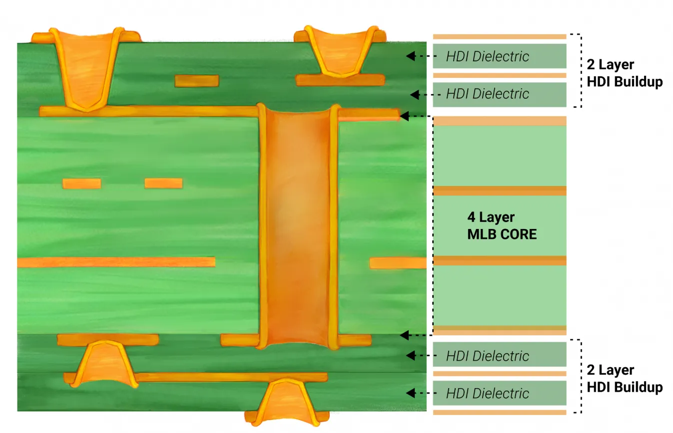
6 layer HDI PCB manufacturing uses sequential lamination of cores and prepregs. Laser drilling creates microvias in outer layers. Plasma desmear prepares via surfaces before copper plating.
Electrolytic plating fills microvias to ensure reliable connections. Multiple registration steps control layer alignment.
Surface finish selection balances solderability and shelf life. Process controls monitor plating thickness and via fill quality. Cross-section analysis verifies structural integrity at critical stages.
Manufacturing Order Profile
| Order Quantity | Order Proportion | Estimated Price Level | Typical Lead Time |
|---|---|---|---|
| Prototype (<=30 pcs) | 71% | From $210 | From 8 days |
| Small volume (30-200 pcs) | 19% | From $240 | From 8 days |
| Mass production (>200 pcs) | 10% | From $350 | From 10 days |
Manufacturing Challenges & Process Optimization
Design Considerations
Related Products
.webp)
Common Applications
PCB Solution for Telecommunication
AIVON telecommunication PCBs are high-performance boards designed for fast and stable signal transmission. Used in base stations, routers, satellite systems, and 5G infrastructure, they feature advanced materials and precision manufacturing to ensure low signal loss, accurate impedance control, and reliable high-frequency performance.
PCB Solution for Medical Devices
AIVON medical device PCBs are high-reliability boards designed for healthcare applications. Built with strict quality control, biocompatible materials, and precise manufacturing, they ensure safety and accuracy. Suitable for diagnostic equipment, patient monitoring, and wearable medical devices, AIVON PCBs meet ISO and IPC medical standards.
PCB Solution for Aerospace and Aviation
AIVON provides high-reliability PCBs designed for civil aviation and aerospace applications, built to perform under extreme conditions such as vibration, temperature variation, and high-altitude environments. These PCBs are widely used in avionics systems, flight control modules, communication equipment, and satellite technologies. With advanced multilayer structures, heavy copper options, and high-temperature materials, our solutions are engineered to meet stringent reliability standards such as IPC-6012 Class 3.
Real Production Records
| Order ID | PCB Type | Layers | Dimensions | Solder Mask | Surface Finish | Quantity | Action |
|---|---|---|---|---|---|---|---|
| Loading... | |||||||
View More Engineering Resources
Why Choose AIVON for 6 Layer HDI PCB?
AIVON produces 6 Layer HDI PCB with advanced sequential lamination, laser-drilled microvias, and tight layer-to-layer registration control, ensuring complex interconnect reliability, signal integrity stability, and consistent high-yield mass production.
The Impact of Microvias on HDI PCB Performance: A Comprehensive Analysis
Discover how microvias transform HDI PCB performance through superior signal integrity, higher routing density, and better reliability. Explore impedance control, current capacity, stacked microvia design rules, challenges, and best practices per IPC standards for high-speed electronics.
Read More
Troubleshooting Common HDI PCB Problems: A Practical Guide
Learn practical solutions with this HDI PCB troubleshooting guide. Identify and fix common defects like microvia failures and signal issues. Perfect for electrical engineers seeking reliable failure analysis tips.
Read More


