Introduction
High-density interconnect (HDI) printed circuit boards represent a critical advancement in modern electronics, enabling compact designs for applications ranging from smartphones to medical devices. Microvias play a pivotal role in HDI PCBs by providing precise interlayer connections that support finer pitch components and higher routing densities. These small vias, typically laser-drilled with diameters under 150 microns, allow for reduced layer counts and shorter signal paths compared to traditional through-hole vias. However, their integration introduces unique challenges in performance metrics such as signal integrity, thermal management, and mechanical durability. This analysis explores how microvias influence key aspects of HDI PCB performance, including microvia impedance, microvia reliability, microvia current carrying capacity, microvia design rules, and the use of stacked microvias. Engineers designing HDI boards must balance these factors to achieve optimal functionality and manufacturability.
What Are Microvias and Why Do They Matter in HDI PCBs?
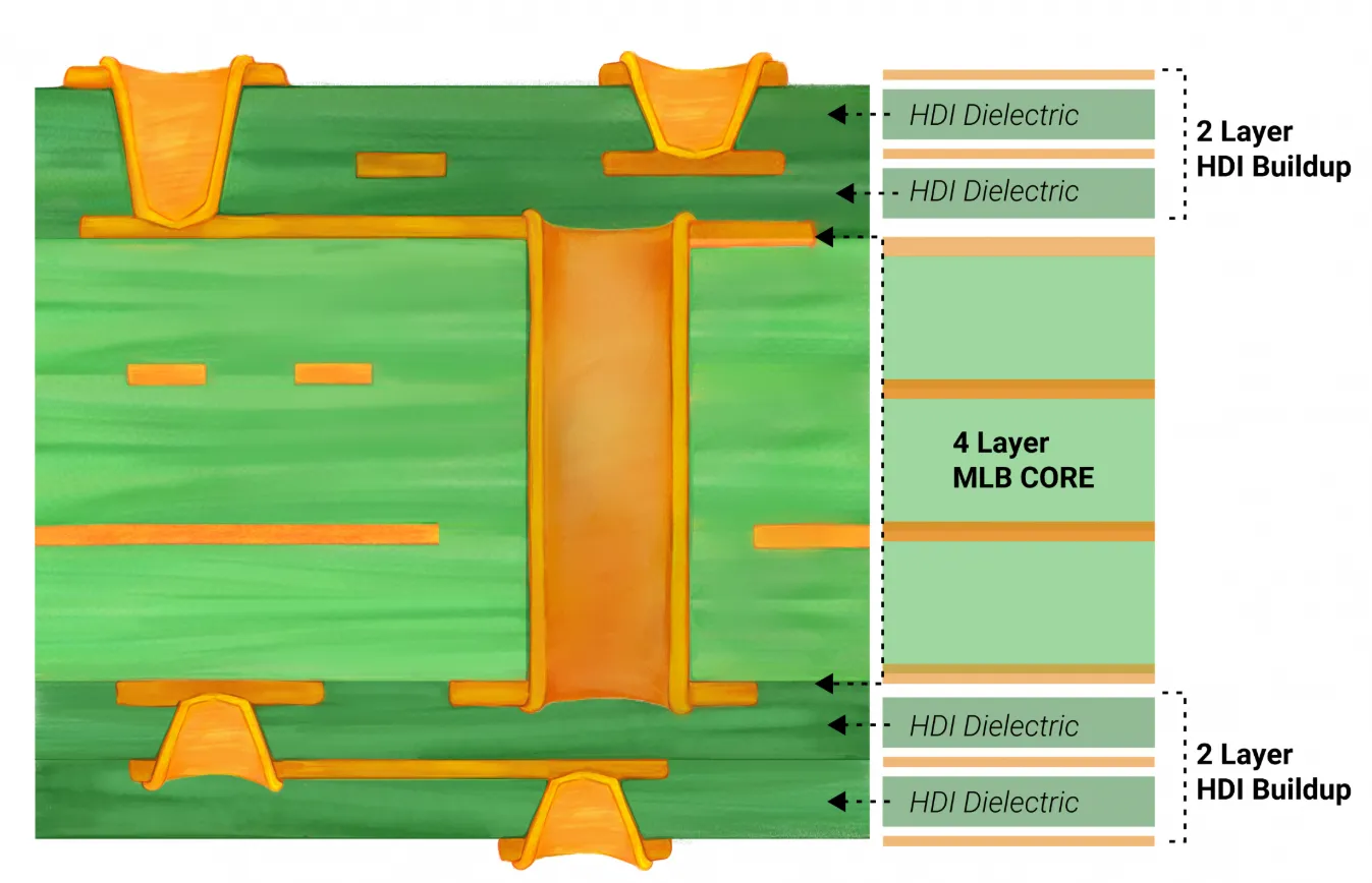
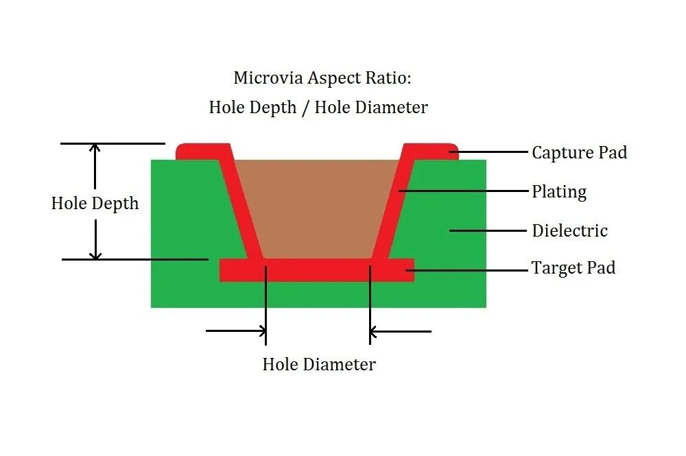
Microvias are blind or buried vias with small aspect ratios, generally defined by industry terminology as structures with a maximum aspect ratio of 1:1 and a total depth not exceeding 0.25 mm. In HDI PCBs, they enable higher interconnect density by connecting adjacent layers without penetrating the entire board stackup, thus minimizing via stubs that degrade signal quality. This capability supports build-up processes where sequential lamination adds layers with embedded microvias, facilitating finer trace widths and spaces down to 50 microns or less. The relevance of microvias stems from the demand for miniaturization in high-performance electronics, where conventional vias limit routing efficiency and increase board size. Without microvias, achieving the density required for advanced BGAs or chip-scale packages becomes impractical. Their adoption directly impacts overall HDI PCB performance by enhancing electrical efficiency while posing risks in reliability if not properly engineered. For deeper insight into HDI stackup construction, see our guide on Sequential Lamination in HDI PCBs: The Definitive Guide to Blind and Buried Vias.
Microvias vs Traditional Vias: Key Performance Differences
Traditional through-hole vias are mechanically drilled and span the entire board thickness, while microvias are laser-drilled and layer-specific. This fundamental difference drives major performance gains in HDI designs.
Comparison Table:
| Aspect | Microvias | Traditional Through-Hole Vias |
|---|---|---|
| Diameter | ≤150 μm (typically 50–100 μm) | 200–1000 μm or larger |
| Aspect Ratio | ≤1:1 (preferred 0.75:1) | Often 5:1 to 10:1 or higher |
| Manufacturing | Laser drilling | Mechanical drilling |
| Layer Connection | Adjacent or limited layers (blind/buried) | All layers (through entire stack) |
| Signal Integrity | Lower inductance/capacitance; shorter paths, fewer stubs | Higher parasitics; longer stubs cause reflections |
| Routing Density | Significantly higher (4–8x in HDI) | Limited by large size and stubs |
| Thermal/Mechanical Stress | Concentrated at neck; sensitive to stacking | More robust but occupies more space |
| Best For | High-speed, high-density, compact designs | Power distribution, low-density boards |
Microvias excel in signal integrity for gigabit+ applications due to reduced parasitic effects, while traditional vias remain useful for high-current or structural connections where space allows.
Microvia Impedance Control in HDI Designs
Microvia impedance becomes a critical concern in HDI PCBs operating at high frequencies, as these vias introduce discontinuities that can cause signal reflections if not managed. The shorter length of microvias reduces inductive reactance compared to through vias, but transitions at the via pad and anti-pad must maintain consistent characteristic impedance, typically 50 ohms single-ended or 100 ohms differential. Engineers achieve control through precise stackup planning, where dielectric thickness and material properties align with trace geometry to minimize mismatches. Laser-drilled microvias, often filled or plated, exhibit lower parasitic capacitance due to their reduced diameter, aiding high-speed signal propagation. However, in dense routing, adjacent microvias can couple crosstalk, necessitating guard traces or ground planes for isolation. Proper impedance modeling during design verification ensures microvia transitions do not compromise the eye diagram or bit error rates in gigabit applications.
Factors Affecting Microvia Reliability
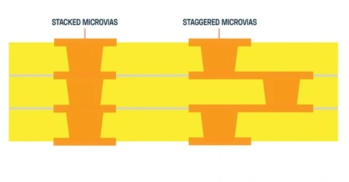
Microvia reliability hinges on several interrelated factors, including plating integrity, thermal cycling, and mechanical stress from coefficient of thermal expansion (CTE) mismatches between copper and dielectrics. During fabrication, electroless and electrolytic plating must fill the microvia uniformly to prevent voids that lead to electromigration under current stress. Reliability testing reveals that stacked microvias experience higher stress concentrations at interfaces compared to staggered configurations, potentially accelerating crack propagation. Adherence to performance specifications like IPC-6012 helps qualify boards by defining acceptance criteria for via integrity after thermal shock and accelerated life tests. Material selection, such as low-CTE resins, further bolsters endurance by reducing shear forces at via barrels. In field use, microvia reliability directly influences HDI PCB lifespan, with failures manifesting as open circuits in high-reliability sectors like aerospace.
Microvia Current Carrying Capacity Considerations
The current carrying capacity of microvias limits their use in power distribution nets within HDI PCBs, primarily due to their smaller cross-sectional area and thinner plating compared to standard vias. Plating thickness, typically 15-25 microns, determines the effective copper fill, with thermal rise dictating safe operating limits based on ambient conditions and adjacent heat sources. In high-current paths, multiple microvias in parallel compensate for individual limitations, but this increases density and potential for thermal hotspots. Engineers must model joule heating effects, considering via depth and dielectric thermal conductivity to avoid exceeding 10-20 degree rises under load. Copper-filled microvias offer improved capacity over plated-only structures by providing solid conduction paths and better heat dissipation. Balancing microvia current carrying capacity with signal vias ensures HDI designs support both logic and power demands without derating.
Microvia Design Rules and Stacked Microvias
Microvia design rules form the foundation of robust HDI PCB layouts, specifying minimum diameters, land sizes, and aspect ratios to ensure drill accuracy and plating uniformity. Guidelines recommend microvia diameters from 50-100 microns with capture and target pads oversized by at least 75 microns to accommodate registration tolerances. Stacked microvias, where one via sits directly atop another across sequential layers, enable direct vertical interconnects but demand tighter process controls due to accumulated misalignment risks. In contrast, staggered microvias offset each via, distributing stress and easing fabrication, though they consume more horizontal space. Standards like IPC-2226 outline these rules, including maximum stack heights of 3-4 microvias to maintain yield. Adhering to microvia design rules prevents common pitfalls such as dog-boning or breakout failures during sequential lamination. When stacking is required for maximum density, review Stacked Microvias: Enabling High Density Interconnects for Advanced Electronics.
Best Practices for Optimizing Microvia Performance
Implementing best practices begins with stackup optimization, selecting laser-drillable dielectrics with uniform ablation rates to achieve clean microvia walls. During design, simulate microvia transitions using field solvers to predict impedance and crosstalk, iterating pad geometries for optimal back-drill equivalents. Fabrication partners should employ plasma cleaning prior to plating to enhance adhesion and reduce voids, critical for microvia reliability. For stacked microvias, limit configurations to two levels unless qualified for higher classes, and incorporate filled vias for power applications to boost current carrying capacity. Post-fabrication, cross-section analysis verifies plating thickness and barrel quality per IPC acceptance criteria. These steps collectively elevate HDI PCB performance, minimizing field failures and supporting higher yields.
Challenges and Troubleshooting in Microvia Integration
Common challenges in microvia integration include via cratering from resin smear during lamination and cracking under reflow due to CTE differentials. Troubleshooting involves desmear processes optimized for microvia scales, using permanganate etching to remove residues without enlarging holes. Signal integrity issues from microvia stubs arise in unfilled structures, resolvable by back-drilling or filling with conductive epoxy. Reliability data from thermal cycle tests highlights stacked microvias' vulnerability, prompting shifts to staggered where density permits. Current bottlenecks manifest as voltage drops, addressed by paralleling vias or upgrading to filled types. Systematic root-cause analysis, guided by design rules, resolves these to sustain HDI performance. Common defects like voiding and delamination are covered in detail in Troubleshooting Microvia PCB Defects: A Guide to Identifying and Resolving Common Issues.
Applications and Case Studies in Modern Electronics
Microvias power HDI success across industries:
- Smartphones and Wearables: Enable ultra-compact boards with any-layer interconnects, fine-pitch processors, and camera modules.
- 5G and Telecom: Support mmWave modules and high-speed routing with minimal signal degradation.
- Medical Devices: Facilitate miniaturization in implants, wearables, and imaging systems where reliability is critical.
- Automotive/ADAS: Provide robust interconnects under vibration and thermal extremes for radar, infotainment, and control units.
- Aerospace: Deliver high-density, lightweight solutions meeting stringent qualification standards.
Case examples show HDI with stacked/staggered microvias reducing board size by 30–50% while improving signal performance and thermal margins in real deployments.
Cost-Benefit Analysis and When to Use Microvias
HDI with microvias increases fabrication complexity and cost (sequential lamination, laser drilling, tighter tolerances) compared to standard PCBs—often 20–100%+ premium depending on type and volume. However, benefits frequently outweigh costs through reduced layer count, smaller form factor, lower material usage, improved performance, and fewer system-level issues.
Use microvias when:
- Component density or fine-pitch packages demand it.
- High-speed signals require minimized stubs and parasitics.
- Size/weight constraints are critical (portables, wearables).
- Reliability targets justify investment in controlled processes.
For lower-density or cost-sensitive designs, hybrid approaches (mixing microvias with standard vias) or traditional boards may suffice. Early cost modeling and DFM reviews help balance trade-offs.
Conclusion
Microvias profoundly shape HDI PCB performance by enabling density unattainable with legacy vias, yet their success depends on meticulous control of impedance, reliability, and current capacity. Key insights include prioritizing low-aspect ratios and robust plating for endurance, staggered over stacked where feasible, and simulation-driven design rules for integrity. Engineers benefit from structured approaches that align fabrication capabilities with application demands, ensuring compact, reliable boards. As HDI evolves, mastering microvia nuances will drive innovation in high-performance electronics. Adopting these principles yields boards that excel in speed, durability, and efficiency.
FAQs
Q1: What factors most influence microvia impedance in HDI PCBs?
A1: Microvia impedance depends on pad geometry, dielectric thickness, and plating quality, with shorter via lengths reducing inductance but requiring precise anti-pad sizing to avoid reflections. Simulations help match trace impedance, typically 50 ohms, while minimizing crosstalk from dense arrays. Following microvia design rules ensures transitions maintain signal integrity at multi-GHz speeds.
Q2: How does microvia reliability differ between stacked and staggered configurations?
A2: Stacked microvias concentrate stress at interfaces, demanding superior plating for thermal cycling endurance, while staggered distribute loads better, easing fabrication. Both benefit from low-CTE materials and aspect ratios under 1:1. IPC-6012 criteria guide qualification to prevent electromigration failures.
Q3: What determines microvia current carrying capacity?
A3: Capacity stems from copper cross-section, plating thickness, and thermal environment, with filled microvias outperforming plated ones for power nets. Paralleling vias compensates limitations, but modeling prevents overheating. Design rules cap rises to maintain reliability.
Q4: Why are microvia design rules essential for HDI performance?
A4: Rules dictate diameters, lands, and stacking to ensure alignment and plating, preventing voids or opens. Stacked microvias need stricter tolerances than staggered. Compliance boosts yield and supports high-density routing without compromising impedance or reliability.
References
IPC-T-50M — Terms and Definitions for Interconnecting and Packaging Electronic Circuits. IPC.
IPC-2226A — Sectional Design Standard for High Density Interconnects. IPC.
IPC-6012D — Qualification and Performance Specification for Rigid Printed Boards. IPC, 2015.


