Introduction
Fine Pitch Technology (FPT) refers to PCB assembly processes for integrated circuit packages featuring lead spacings of 0.65 mm or less. This technology accommodates high pin count components essential for compact, high-performance electronics. However, using FPT introduces complex challenges in manufacturing, assembly, and testing that demand precise engineering controls. Engineers encounter issues like solder defects, alignment errors, and probing difficulties, particularly with high pin count devices. Addressing these challenges ensures reliable performance and yield in production. This article details the primary obstacles and best practices for overcoming them.
What Is FPT and Why It Matters
FPT encompasses surface mount technologies for components such as Quad Flat Packages (QFPs), Thin Quad Flat Packages (TQFPs), and Ball Grid Arrays (BGAs) with pitches down to 0.4 mm in advanced designs. It matters because modern electronics require higher integration to meet demands for smaller form factors and faster signal speeds. High pin count components under FPT enable this density but amplify risks in assembly processes. Without proper management, defects can lead to field failures and increased costs. Industry standards like IPC-7351 provide guidelines for land pattern design to mitigate these risks. Ultimately, mastering FPT is crucial for electric engineers designing next-generation PCBs.
Key Technical Challenges in Solder Paste Application
Applying solder paste uniformly on fine pitch pads poses significant hurdles due to the reduced spacing between pads. Stencils must feature apertures smaller than 0.3 mm, which increases the risk of insufficient paste volume or smearing. Variations in paste viscosity or printing pressure exacerbate these issues, leading to inconsistent deposits. For high pin count components, even minor inconsistencies can result in opens or bridges during reflow. Printer alignment tolerances tighten to sub-25 micron levels to prevent offsets. Engineers must optimize stencil thickness, typically 0.1 mm for FPT, to balance paste release and resolution.
Component Placement Precision Issues
Placement accuracy is critical in FPT, where component leads or balls occupy spaces as small as 0.2 mm. Pick-and-place machines require vision systems capable of 10-micron repeatability to align components correctly. High pin count devices amplify errors, as misalignment on one side propagates across the package. Board warpage further complicates placement, causing coplanarity issues between component and PCB. Self-alignment during reflow helps but fails if initial offset exceeds 25% of pitch. These challenges demand advanced fiducials and machine calibration for consistent results.
Reflow Soldering Defects and Thermal Management
Reflow soldering in FPT often results in defects like bridging, tombstoning, or head-in-pillow effects due to the fine geometry. Solder bridges form when excess paste merges between adjacent pads under surface tension. High pin count increases the probability, as inner rows receive uneven heating. Thermal profiles must ramp slowly to avoid voids, per J-STD-001 requirements for soldering processes. Component warpage or PCB bow exceeds 0.75% in some cases, disrupting joint formation. Profile optimization using thermocouples ensures peak temperatures align with alloy melting points without overheating.
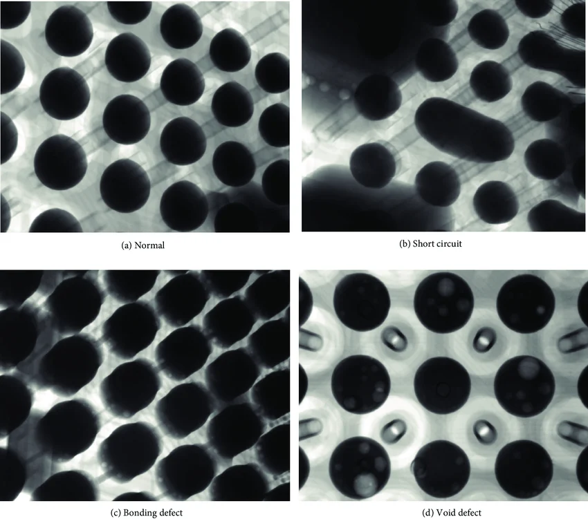
Inspection and Rework Difficulties
Visual inspection of FPT assemblies challenges automated optical inspection (AOI) systems due to shadow effects from dense leads. X-ray becomes essential for hidden joints in BGAs, but interpreting images for high pin count arrays is time-intensive. Rework involves precise desoldering to avoid pad lifts or trace damage. IPC-A-610 criteria define acceptable joint criteria, such as heel fillet height and wetting, but fine pitches make compliance verification subjective. Manual rework risks contamination or ESD damage. These factors extend cycle times and raise costs in production.
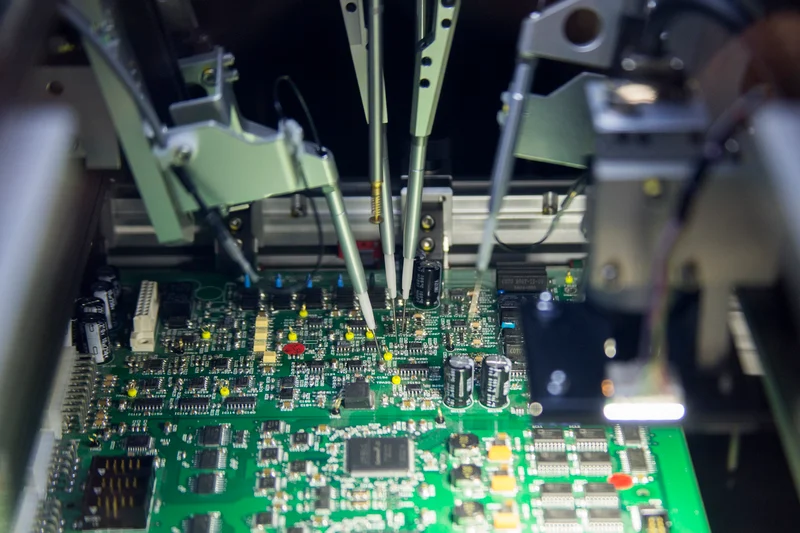
Testing Challenges with High Pin Count Components
Component testing in FPT PCBs encounters probing limitations for fine pitches and high pin counts. Traditional bed-of-nails fixtures become impractical due to the density, requiring thousands of probes with 0.1 mm spacing. Flying probe testers offer flexibility but slow throughput for high pin count nets. Electrical continuity tests risk shorts if probes slip, and functional testing demands custom interfaces. High pin count exacerbates crosstalk during in-circuit testing, complicating measurements. Standards like IPC-9252 guide test point design, but access remains a bottleneck.
Signal Integrity and Routing Constraints
FPT designs impose routing challenges for high-speed signals amid fine lines and spaces below 0.1 mm. Impedance control becomes difficult with reduced trace widths, leading to reflections or attenuation. High pin count escape routing from inner balls consumes layers, increasing via density. Crosstalk rises between adjacent fine traces without sufficient ground planes. Engineers must employ differential pairs and length matching per IPC-2221 guidelines. These issues degrade performance in RF or high-frequency applications.
Practical Solutions and Best Practices
To counter solder paste challenges, use laser-cut or electroformed stencils with nano-coatings for clean release. Implement step-printing for mixed pitch boards to optimize volumes. For placement, integrate 3D vision systems and employ board support to minimize warpage. Reflow ovens with multi-zone control allow tailored profiles, verified by real-time monitoring. Adopt 100% AOI supplemented by X-ray for inspection, focusing on IPC-A-610 Class 3 criteria for critical joints. In testing, combine flying probes with boundary scan for high pin count efficiency, ensuring test coverage exceeds 95%.
Design land patterns per IPC-7351 to promote self-alignment and robust joints. Simulate thermal profiles early to predict defects. Select low-warpage substrates and controlled baking to manage moisture. For rework, use convection hot air tools with flux dipping for precision. Collaborate across design, fabrication, and assembly teams for design-for-manufacturability (DFM) reviews. These practices reduce defect rates below 500 DPMO in FPT production.
Troubleshooting Common FPT Failures
Engineers often troubleshoot bridging by analyzing paste volume and stencil snap-off speed. Opens trace back to insufficient paste or oxidation, resolved by nitrogen reflow atmospheres. Warpage failures require shadow moiré analysis to quantify bow. High pin count test fails stem from fixture misalignment, addressed by CAD-to-fixture verification. Component testing issues like probe marks on fine pads demand softer tips or flying probes. Systematic root cause analysis using fishbone diagrams guides corrections.
Conclusion
Using FPT unlocks high density and performance but demands mastery of precision processes. Challenges in paste application, placement, soldering, inspection, and especially component testing for high pin count devices require rigorous controls. Adhering to standards like J-STD-001 and IPC-A-610 ensures quality. Best practices in design, simulation, and process optimization yield reliable assemblies. Electric engineers benefit from proactive DFM to navigate these hurdles effectively. Future advancements in automation will further ease FPT implementation.
FAQs
Q1: What are the main challenges in component testing for high pin count FPT PCBs?
A1: High pin count FPT boards complicate fixture design for in-circuit testing, as probe spacing limits access to fine pitches. Flying probe systems provide flexibility but reduce speed for thousands of nets. Electrical noise from dense routing affects measurements. Best practices include boundary scan integration and optimized test point placement to achieve high coverage without physical damage.
Q2: How does high pin count impact using FPT in assembly?
A2: High pin count amplifies risks of misalignment and uneven reflow in FPT, leading to joint defects across the package. Escape routing consumes board real estate, raising layer counts. Testing throughput drops with traditional methods. Solutions involve precise placement machines and layered stackups designed per IPC-7351 for reliable fanout.
Q3: Why is solder bridging common when using FPT?
A3: Solder bridging occurs in FPT due to capillary action pulling excess paste between close pads during reflow. Fine apertures deposit more paste relatively, worsening the issue. High pin count inner rows heat unevenly. Mitigate with volume-controlled stencils, optimized profiles, and post-print inspection to prevent bridges.
Q4: What role do standards play in overcoming FPT challenges?
A4: Standards like IPC-A-610 define joint acceptability, guiding inspection criteria for fine pitch defects. J-STD-001 specifies soldering parameters to minimize voids and bridges. They ensure consistency across processes, from land design to testing, reducing variability in high pin count assemblies.
References
IPC-7351B — Generic Requirements for Surface Mount Design and Land Pattern Standard. IPC, 2010
IPC-A-610H — Acceptability of Electronic Assemblies. IPC, 2019
J-STD-001G — Requirements for Soldered Electrical and Electronic Assemblies. IPC, 2011